Electromagnetic Interference
13/09/2021, hardwarebee
The prime objective of any electronic circuit is to perform a specific function. Therefore, the main goal of a designer is to achieve this function in the most efficient and safe way. However, one aspect that is often overlooked during early design, and that is as important as the circuit’s main function, is the electromagnetic interference. The electromagnetic fields (EF) present in the air can be coupled, which results in noise and malfunctioning. On top of that, the EF generated by the device will interfere with the surrounding equipment, especially if the circuit works with high frequencies. Therefore, the device should be isolated from external EF fields while not interfering with nearby equipment. In that sense, two quantities should be addressed during early design: the electromagnetic interference (EMI) and the electromagnetic compatibility (EMC). Engineers should consider both EMI and EMC not only to improve the product, but also because electronic devices must be approved and certified by regulatory agencies before being commercially released.
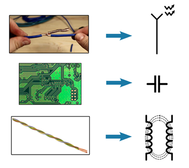
Figure 1: Radiated, capacitive and inductive EMI and the respective real-life cases
WHAT IS ELECTROMAGNETIC INTERFERENCE?
Electromagnetic interference (EMI) is the unwanted electromagnetic energy that reaches a device and causes malfunction. This malfunction usually occurs in the form of noise, but other problems can also occur, such as communication errors in HF devices and measurement errors in instrumentation electronics. One classic EMI signal is the 50/60 Hz signal (the frequency varies with the country) coupled from the power lines that can be found in instrumentation devices, especially when lacking proper filtering.
Electromagnetic interference (EMI) exists in two basic ways: radiated emission and conducted emission. Radiated emission occurs when energy is transferred through the air, via electromagnetic waves. This radiation can be generated by AM and FM transmitters, WiFi antennas, Bluetooth communicators, and basically any circuit operating in high frequencies, due to antenna effects in the PCB. Conducted EMI is transmitted via wires and cables, existing in the power networks, ground lines, metal housing, etc.
ELECTROMAGNETIC COMPATIBILITY
Electromagnetic compatibility (EMC) is a quantification of the harmonic operation between the device and the surrounding electromagnetic field. That is, how compatible the equipment is with the rest of the equipment in terms of EMI. Whereas EMI considers only the interference itself, EMC deals with the whole context of application: how much does my device affects and is affected by the rest of the equipment?
For a device to be compatible with a certain environment, two things should be considered: the amount of EMI generated by the device, and the amount of immunity to external EMI. Both deal with the radiated and conducted interference. For instance, in a medical environment there is a certain level of EMI, if the level of electromagnetic immunity of the new device is lower than the external EMI, the device will present malfunctioning in such environment and will not pass the EMC certification.
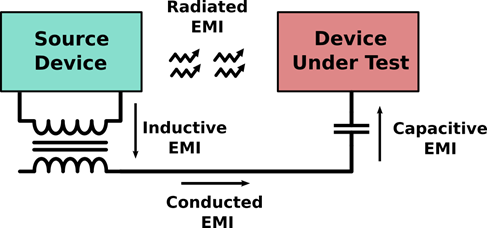
Figure 2: All sources of radiated and conductive EMI, including inductive and capacitive coupling.
REGULATIOM
As stated before, in order to prevent device malfunction and to ensure that every environment present a predictable level of EMI, national and international standards for EM interference and immunity were defined. Globally, the IEC (International Electrotechnical Commissions) establishes both interference and immunity standards for new devices that are adopted by many countries, such as the US, Japan, Taiwan and Europe nations. However, even in these countries, the legislation may vary, so developers must check the specific legislation of the target market.
To verify what standards and tests that should be met for a specific product, the designer should first identify the regulatory agency that is responsible for the device type. For instance, in the US biomedical products are regulated by the FDA (Food and Drug Administration), and communication devices are regulated by the FCC (Federal Communications Commission). These agencies define the regulations that the devices must meet via EMI/EMC testing.
EMI SHIELDING
One of the most frustrating situations during a design is getting a certification refused after months of work. Also, EMI/EMC tests are expensive, so failing one or more tests could increase significantly the development cost of the project, besides the additional cost of making changes in the product at the end of the design cycle. Therefore, it is important to verify if your device complies with the EMI/EMC regulations of the target market during the early stages of design. Here we present some EMI Shielding tips to improve the EMI emission and immunity of your electronic device, based on the IEC regulations and basic electromagnetic theory.
PACKAGE SHIELDING
Electromagnetic waves can be absorbed by metal sheets when connected to ground. The EM generates a current within the metal sheet, which is then absorbed by the ground connection. The EMI energy is then consumed as heat. If a box made of metal sheets is built around a device, both EMI generated by the device and the external EMI are isolated from each other. Therefore, package shielding is able to increase the radiated EM immunity and emission of a device. This is known to improve the compatibility of the equipment significantly, and depending on the design may be enough to isolate radiated electromagnetic fields. The main advantage of this technique is that it can be implemented by the end of design flow, which can save the design if the equipment itself does not comply with EMI/EMC requirements. However, it is often bulky and does not protect against conducted EMI.
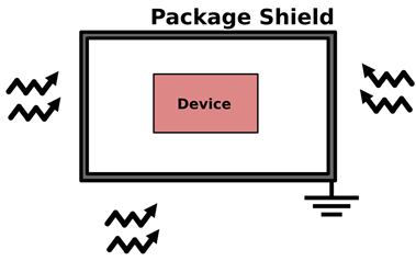
Figure 3: Package shield protecting a device from external EMI
CABLE SHIELDING
A cable is a problem connecting two other problems, so care should be taken when designing the cable system for sensitive EMI devices. Because of its long shape, cables can act as antennas, coupling radiated electromagnetic waves from the surroundings. Also, inductive and capacitive coupling can occur with nearby equipment.
One way to prevent this problem is using cable shielding. The principle is the same as the package shielding: a grounded metal foil surrounding the main line. The shield isolates the main line from the external field, increasing EM immunity and the emitted EMI. Shielded wires are typical, but sensitive signals (such as in instrumentation systems) require coaxial cables. Both shielded wires and coaxial cables increase the capacitance of the transmission line, which may degrade the signal in high frequencies. In these cases, triaxial cables may be the best choice, with an intermediary shield that is driven with the same voltage as the main line. In this case, the main line is isolated from the grounded shield, eliminating the capacitance.
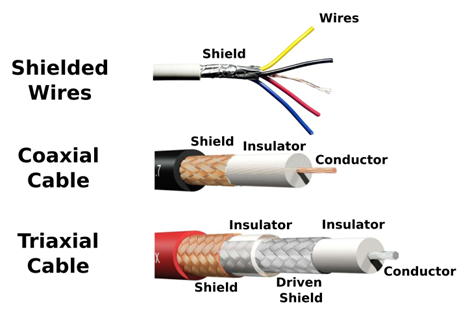
Figure 4: Shielded wires, coaxial cables and triaxial cables
DIFFERENTIAL SIGNALING
If cables as too close to each other, the noise generated by external EMI coupling will be similar. Therefore, the differential voltage between these two cables that emerges from this EMI will decrease with the approximation of the cables. If the cables are ideally close together, the EMI coupled in the differential voltage will be zero. Therefore, one way of reducing the effects of external EMI is to twist two cables and transmit information using the differential voltage between these cables, instead of the single-ended voltage (referenced to ground).
This technique provides even more advantages: first, the conducted EMI that is coupled in the ground paths is eliminated, because the signal is no longer referenced to the ground. Second, the voltage compliance is doubled, so lower voltage devices can be used and the SNR increases. Finally, the radiated EMI generated b the device is reduced, because each cable transmits the opposite current, which cancels the emitted field. Differential signaling is not limited to cables, and can be used in low voltage PCBs with similar characteristics. One important note is that the paths must be as close and identical as possible, to avoid mismatches. One classic standard is the LVDS (Low Voltage Differential Signaling), which is implemented in low voltage signal transmission in differential lines. The main drawback of differential signaling is the need for fully differential amplifiers and signal processing units, which increases complexity and, consequently, cost.
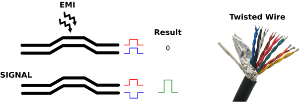
Figure 5: The advantages of differential signaling and the twisted wire
POWER LINE FILTER
Conducted EMI is transmitted between different equipment through the power line. The power line can couple significant amounts of EMI, and if the PSRR (Power Supply Rejection Ratio) is not good enough, this interference gets coupled into the device. The most basic way to prevent sensitive signals to get corrupted is to implement a power line filter. Line filters are devices that isolate the power line from the device, allowing only the power signal to pass. It usually implements a differential filter, tuned in 50/60 Hz (depending on the power system) and a common-mode filter, which allows only differential currents to pass. The common-mode filter consists of two inductors sharing a core, called EMI choke. Both inductors are wired in the same direction, so the common-mode current adds flux to the core, acting as a high impedance inductive path, and the differential current cancels each other flux, acting as a low impedance path. Power line filters are fundamental to prevent conducted EMI, and can improve significantly the EMI/EMC compliance of a device.
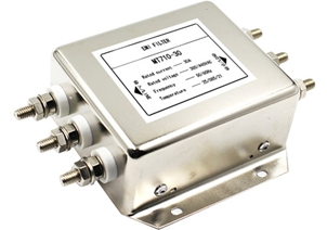
Figure 6: A commercial power liner filter
GROUND AND POWER PLANES
Finally, at the PCB level, EMI can be reduced by proper grounding. To avoid pick-up noise, ground and power paths should be as small as possible. Also, it should not form loops. Ground loops in high frequency systems are basically antennas, picking up and sending EMI to nearby devices. The most efficient way of reducing the chance of ground loops is to implement ground planes. Ground planes are entire layers of grounded copper sheets that allows current flow through the smallest paths, decreasing the chance of noise pick-up and emission. The same goes to power planes in PCB. This technique has the additional advantage of providing EMI shields for the PCB, absorbing radiation before it reaches the signal layers. Therefore, power and ground layers are essential to obtain a good EMI/EMC compliance, and should be implement whenever is possible.

Figure 7: Ground plane for double-layer PCB and power/ground layers for triple layer PCB
EMI/EMC TESTING
EMI/EMC testing should cover both the immunity testing, which tells how much the device is affected by external fields, and emission testing, which tells how much the device generates EMI. The specific test that should be applied depends on the nature of the device under test and the regulatory requirements of the legislation responsible for it. For instance, for medical devices the FDA requires that the tests should cover the FDA Reviewer Guidance document, and the Europe Union requires that the European IEC 60601-1-2 standards should be satisfied.
The tests can check the EMC compliance concerning magnetic fields, power interruption fluctuations, electro- static discharges, EM noise, surges caused by lightning, high speed switching signals, etc. The job of an EMC testing laboratory is to simulate all these extreme conditions to check if the device still works properly. Also, it should measure the amount of EM emitted by the device to verify if it complies with the EMI standards. Only if the device passes all tests, it gets certified to be released to the market.


