Understanding Oscilloscope Probes
29/05/2023, hardwarebee
Oscilloscope is considered one of the crucial tools when working on electronic circuits. It shows vital information about the circuit connected to it and displaying different waveform parameters.
An oscilloscope probe is a device that makes a physical and electrical connection between an oscilloscope and DUT. There is no other way to connect an oscilloscope and your circuit without a probe. The selection of a probe is also an important task, because your circuit measurements are dependent on the probe performance. So, the presence, quality, and selection of the probe matter a lot in the phase of debugging a circuit.
One end of the probe is connected to the probed circuit, and the other end is connected to the oscilloscope. After connecting a probe, it becomes part of your circuit. It may adversely affect the behavior of your circuit like interference, loading effect, and signal fidelity. They are designed to counteract these unwanted effects.
The upcoming paragraphs will address various realities that hinder practical probes from attaining the ideal state.
Physical Connection
The initial step involves establishing a connection with the test point. Gently touch the probe tip to the desired test point in the circuit to establish the signal connection. It is important to ensure that the probe tip makes secure and reliable contact with the test point. Select a lightweight and compact probe with a tip that is compatible with the test point, especially in the case of surface-mount technology (SMT).
These probes are not suitable for industrial applications, which often involve high-power circuitry and larger gauge wires. In such cases, larger probes capable of measuring high voltages are available. Consequently, a variety of probe sizes and configurations have been developed to meet the physical connection demands of different applications.
Absolute Signal Fidelity
Any practical device never fully achieves idealism. While an ideal probe possesses characteristics such as zero attenuation, infinite bandwidth, and linear phase across all frequencies, real-world probes have limitations.
Therefore, an ideal probe would transmit any signal from its tip to the oscilloscope input and reconstruct it without distortion. However, real probes introduce some level of attenuation, have limited bandwidth, and may exhibit phase distortions at certain frequencies. These factors need to be considered when selecting and using them in practical applications. For accurate signal transfer and fidelity, the probe’s resistance (R) and capacitance (C) should match the input resistance and capacitance of the oscilloscope. Typically, oscilloscopes have an input resistance of 50Ω and 1MΩ. For instance, a 50Ω probe should be utilized with an oscilloscope input of 50Ω, while 1MΩ probes should be employed with scopes possessing a 1MΩ input resistance. The capacitance matching is done through the compensation range of the probe.
Noise Immunity
Multiple potential sources can introduce noise into the signal under test. These sources include the buffer and amplifier circuit within the oscilloscope itself. Additionally, active probes can introduce their noise into the measurement. External sources of noise can also play a role, such as fluorescent lamps and fan motors.
An ideal probe is completely immune to any kind of noise. However, in a practical situation, achieving such immunity is nearly impossible. There are ways to minimize noise and strive for a system that is as noise-free as possible.
Most probes are shielded with coaxial cable, which offers electromagnetic shielding and helps to reduce interference in the measured signal. The coaxial shield, typically constructed from a conductive material, surrounds the signal wire or conductor with a woven metal mesh. The coaxial shield is commonly connected to the ground reference of the oscilloscope, effectively creating a grounded shield around the signal wire.
Loading Effect
When an external device such as a probe is attached to a circuit, it is considered an additional load on that circuit (or signal source), drawing current from the circuit. Assuming the test circuit is a signal source.
An ideal probe has no impact on the circuit under test. It will draw no current or only a little current, therefore causing as little loading effect as possible. In practice, it has resistance, capacitance, and inductance. When a probe is attached to a signal source, it introduces additional resistance, inductance, and capacitance to the circuit, which can alter the behaviour of the source and impact the measurement accuracy.
The probe loading effect can be divided into three categories:
- Resistive loading
- Capacitive loading
- Inductive loading
Resistive Loading
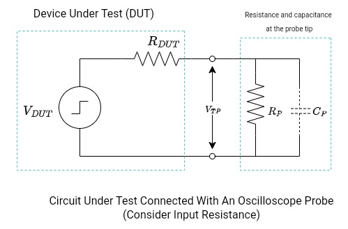
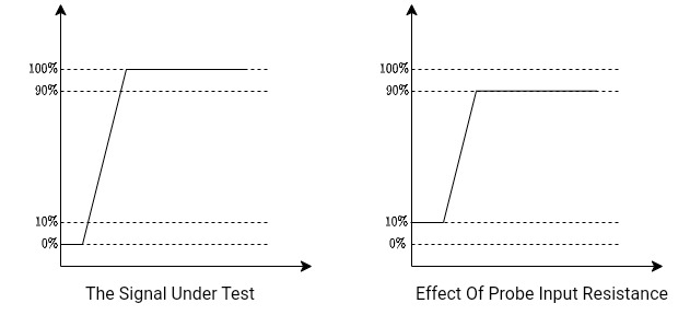
A well-designed probe must have high input resistance. This input resistance appears in parallel with the resistance of the circuit under test.
Suppose,
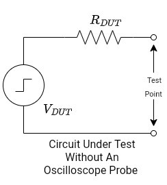
The device under test (DUT) or circuit under test is modeled as VDUT and RDUT.
The probe is modelled as RP and CP, where RP and CP are input resistance and input capacitance, respectively. whereas VTP is the test point voltage.

VTP approximately equals VDUT only, when RP is significantly greater than RDUT. To limit the loading effect, it is advisable to use a probe with a resistance at least 10 times greater than the resistance of the circuit under test. Therefore, the amplitude error could be restricted to 10% only.
Capacitive Loading
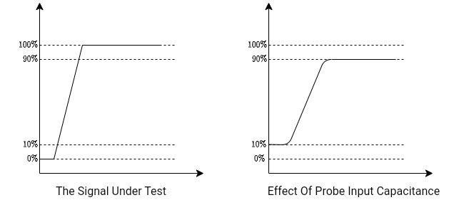
Capacitive loading can be visualized as a capacitor connected in parallel with the circuit being tested. Therefore, the input capacitance of the probe introduces an additional capacitive load. The probe’s input capacitance significantly impacts the behavior of the circuit under test. Capacitive loading becomes more concerning as the frequency increases. With higher test signal frequencies, the probe impedance decreases. This not only affects the signal’s amplitude but also distorts the signal’s shape. To minimize the capacitive loading effect, it is recommended to use a probe with low capacitance, especially for high-frequency applications. This approach helps minimize the adverse impact caused by capacitive loading.
Inductive Loading
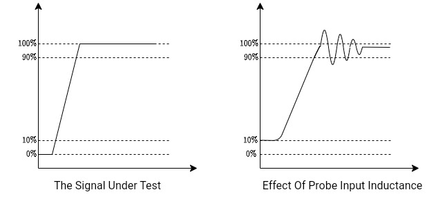
Inductive loading in oscilloscope probes becomes significant at higher frequencies. It occurs due to the probe ground leads. As the frequency of the signal increases, the probe’s inductance and capacitance start to resonate at a particular frequency, which leads to a ringing effect and can cause signal distortion. To mitigate this effect, it is recommended to use the shortest possible ground wire.
Probe Specifications
To perform measurements, the following specifications of an oscilloscope probe should be known. Some of them are listed below.
Attenuation
Attention is referred to as the ratio of the input to the output signal. Probes are available with various attenuation ratios, such as 1:1, 10:1, 100:1, and 1000:1. A 10X probe indicates that the signal applied to the oscilloscope is one-tenth (1/10th) of the actual input signal amplitude. For instance, when a 10:1 probe is connected to a 1-V signal, it will transmit 100 mV to the input of the oscilloscope. The oscilloscope automatically recognizes the probe’s attenuation ratio and displays the accurate signal values on the screen, eliminating the need for mental calculations.
Bandwidth
In general, the bandwidth of an oscilloscope probe should be at least five times greater than the bandwidth of the waveform being measured. It’s important to note that bandwidth is often associated with the -3 dB point, which signifies the frequency at which the signal power is halved (-3 dB) compared to its maximum level.
For a signal with a frequency of 50 MHz, the oscilloscope bandwidth and probe bandwidth must exceed 250 MHz.
BWPROBE > BWWAVEFORM
BWPROBE > = BWSCOPE
Rise Time
To achieve satisfactory precision, the combined rise time of the oscilloscope and its probe should be three to five times greater than the highest rise time of the waveforms being measured.
Measurement system rise time >= signal rise time /5
Input Resistance
It is used to describe the loading effects. The input resistance (probe and oscilloscope) will reduce the amplitude
of the circuit under test.
Input Capacitance (Cin)
This is the input capacitance of the probe, or tip capacitance. Its value is given, but it also depends on the input capacitance of the scope to some extent. Probes with larger capacitance slow down the system’s response.
Maximum Input Voltage (Vmax)
It’s essential to select a probe with an input voltage rating that is appropriate for the voltage levels you’ll be working with. Probes are designed to handle a wide range of voltage levels, allowing them to measure both low and high voltages. The input voltage range of a probe depends on the specific model and type of probe. Typically, passive probes can tolerate several hundreds of volts, while active probes have maximum voltage ratings in the range of a few volts only.
Probe Compensation Range
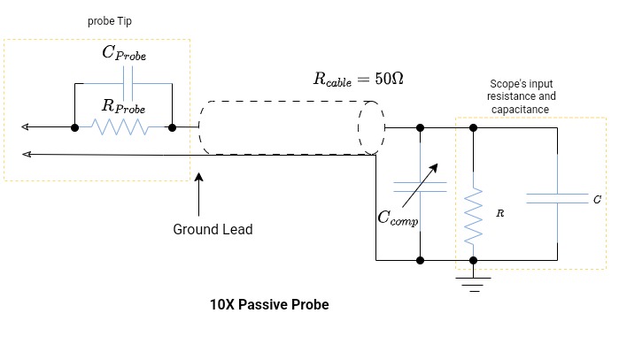
The compensation range is also specific to the probe model, and it is adjustable. There is a trimmer capacitor that allows you to adjust the the probe’s capacitance. It determines the compatibility of the probe with oscilloscopes having varying input capacitance levels within a specified range.
Types Of Probes
Passive Probes
These probes are constructed solely with passive components and do not incorporate any active elements such as transistors or amplifiers. Consequently, there is no need to supply power to the probe. They are widely used due to their user-friendly nature and cost-effectiveness.
To increase the probe resistance, you can simply add a resistor at the probe tip, which will function as a voltage divider.
These probes are specified with various attenuation factors, such as 1X, 10X, 100X, and 1000X. The 10X probe is the most commonly used among them. Additionally, these probes can also be specified by their bandwidth, ranging from 100MHz to 500MHz. It is recommended that the probe’s bandwidth be at least equal to the bandwidth of the oscilloscope.
Active Probes
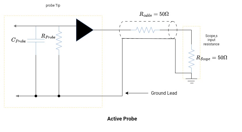
Their functionality relies on active components such as transistors and amplifiers, which exhibit extremely high input impedance and low input capacitance, typically achieved through the use of a FET (field-effect transistor). As a result, active probes require external power to operate. This enables them to amplify signals without drawing power from the circuit under test, effectively reducing the loading effect.
Moreover, active probes exhibit lower input capacitance, which allows them to achieve higher bandwidths ranging from 500 MHz to 4 GHz.
Active probes have an input resistance of either 50 Ω or 1 MΩ, providing a much lower input range compared to passive probes. The input voltage range typically spans from ±0.6 to ±10V, with a maximum voltage range of ±40V.
Switchable Probes
These are suitable when you want to measure a wide range of signal amplitudes. For example a switchable 1X and 10X offer dual attenuation options, that is 1X and 10X
High-Voltage Probes
As the name implies, their purpose is to safely handle high voltage. Passive probes are capable of measuring a maximum voltage of 400 V to 500 V. On the other hand, they can handle maximum ratings of 20,000 V. It is specifically engineered to handle higher voltage levels than standard probes.
These are different from other probes in many aspects. Like,
- They have longer cable lengths, typically 10 feet and 25 feet longer cables.
- They have special insulated ends.
Differential Probes
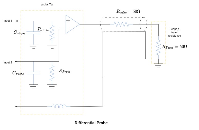
If you need to measure the voltage across different components in a circuit where one or more of these components are not connected to the ground, you need to make differential measurements, and for this, you’ll need a differential probe. It measures the difference between two signals.
Differential signals can be measured by utilizing two single-ended probes and a dual-channel oscilloscope. Conduct two separate, single-ended measurements with respect to the ground reference. Once the two signals have been measured individually, employ the math function of the oscilloscope to calculate the difference between the two signals. This method is suitable for signals with a low frequency and sufficient amplitude.
Differential probes are commonly employed when measuring high-frequency signals or signals with extremely low amplitude. They offer a wider bandwidth, reaching up to 30GHz, low input capacitance (typically less than 1 pF), and relatively high input resistance (usually greater than 50kΩ).

