PCB Stackup: Ultimate Guide and Examples
24/03/2025, hardwarebee
The diversity in PCB stackup types—from standard multilayer to exotic flex and high-density interconnect structures—provides the flexibility to meet varied application requirements. Along with intricate construction methods and critical design tips like selecting the right dielectric materials and ensuring uniform impedance, stackup design is a multifaceted challenge. Tailored approaches can greatly influence the efficiency and longevity of electronic devices in high-tech industries.
This article is your ultimate guide to mastering PCB stackups, offering insightful examples and best practices. From the basics to advanced techniques, we will explore the significance and impact of crucial elements like Ball Grid Array (BGA) components and mechanical requirements. Whether you’re navigating a 4-layer or a 16-layer stackup, this guide sheds light on designing effective stackups tailor-suited to your specific applications.
Importance of PCB Stackup in Electronic Design
PCB stack-up plays a crucial role in electronic design. It refers to the arrangement of copper layers and dielectric materials within a circuit board. The stack-up influences signal integrity, operating frequency, and electromagnetic compatibility.
Key Elements of PCB Stack-up:
- Layer Count: Common configurations include 4, 6, and 8 layer PCB stackups.
- Layers: Includes signal layers, power planes, and ground planes.
- Material: Choice of dielectric materials affects board thickness and impedance.
Proper stack-up helps in thermal management, accommodating flexible materials, and reducing production costs. For mass production, an efficient design ensures consistent performance and reliability.
Benefits of Proper Stack-up:
- Improved Signal Integrity: Carefully arranged layers minimize interference.
- Thermal Management: Helps in heat distribution across metal layers.
- Cost Efficiency: Optimizes the use of materials for budget-friendly mass production.
- Enhanced EMC: Better electromagnetic compatibility with the right layer arrangement.
Using tools like Altium Designer, PCB designers can optimize stack-ups for specific design requirements, ensuring a reliable end product. Remember, sequential lamination and understanding of adjacent signal layers are vital for advanced designs.
Types of PCB Stackups
Understanding PCB stack-ups is vital in electronic design. Different applications and requirements lead to various stack-up types. Choosing the right one impacts the board’s performance and cost efficiency. Common types include standard multilayer, flex and rigid-flex, and high-density interconnect (HDI) stack-up. Each serves distinct purposes in the manufacturing and functionality of circuit boards.
Standard Multilayer Stackup
A standard multilayer stack-up consists of several layers of copper and dielectric materials. These layers include signal, power, and ground layers. This type of stack-up is common in many electronic applications due to its balance of complexity and cost. Multilayer boards usually range from 4 to 8 layers, depending on the design needs.
In a standard stack-up, the outer layers often serve as signal layers, while internal layers are used for power and ground planes. This arrangement helps achieve desired electrical characteristics. The systematic layering supports both signal integrity and thermal management. It also allows adequate routing of signals, contributing to effective circuit board design. Optimal selection benefits mass-produced electronic products by ensuring reliable and consistent performance.
Flex and Rigid-Flex Stackups
Flex and rigid-flex stack-ups combine flexibility and rigidity in one board. This design caters to specific applications requiring bending or movement. They are ideal for compact electronic devices where space is at a premium. In flex stack-ups, the entire board can bend, while rigid-flex types feature both flexible and rigid sections.
These stack-ups involve layers of thin dielectric and copper, which are capable of moving. Using flexible materials brings advantages in weight reduction and space efficiency. This design helps in forming intricate shapes without losing reliability. Additionally, these stack-ups improve wear resistance, accommodating millions of flexing cycles. They are perfect for applications needing high durability and adaptability in designs.
High-Density Interconnect (HDI) Stackup
High-Density Interconnect (HDI) stack-up is key for advanced and complex circuit board designs. It optimizes space by using microvias and fine lines. HDI stack-ups are crucial when integrating numerous electronic components in a small area. They enhance layer density and allow more routing channels, which can support a higher layer count without exponential increase in board thickness.
HDI stack-ups use thin copper layers and finer features. This configuration improves signal integrity and minimizes interference. The precision of HDI also supports higher operating frequencies. Designed for high-performing electronic products, HDI reduces signal loss and improves speed. Simultaneously, it effectively meets design requirements for modern gadgets demanding complex circuitry and space restrictions.
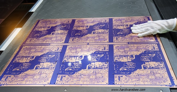
Construction Methods for PCB Stackups
PCB stackup involves arranging layers to achieve the desired electrical and mechanical properties. These layers include signal layers, power planes, and ground planes. The stackup affects the board’s performance, influencing factors such as impedance requirements and signal integrity. PCB stackups play a crucial role in thermal management and electromagnetic compatibility, especially as operating frequencies increase. Two common construction methods are foil construction and cap construction. Each method has its own advantages and is chosen based on design requirements and cost considerations.
Foil Construction
Foil construction is a popular method for creating PCB stackups. This technique involves using sheets of copper foil bonded to dielectric materials. The process begins with the outer layers being laminated with copper foil. This approach allows for greater control over the copper thickness, which is essential for meeting specific impedance requirements and overall board thickness. Foil construction is ideal for high-frequency applications where signal integrity is critical. PCB designers often prefer this method for its flexibility in layer arrangement, which allows for the customization of signal and power layers to suit various electronic products.
In foil construction, the copper layers are adhered directly to the surface layers or embedded in the dielectric materials. This configuration helps in reducing production costs, making it more suitable for mass production. Sequential lamination can be used in this method to add more layers, allowing for complex circuit board designs. Foil construction is often complemented by advanced design software like Altium Designer, which aids in optimizing layer stack-up for improved performance. The outer layers can be adjusted to incorporate flexible materials, enhancing the mechanical durability of the PCB.
Cap Construction
Cap construction is another method used in PCB stackup design. This technique involves pre-manufactured cores with copper on either side. These cores are then bonded with additional outer layers during the lamination process. The primary benefit of cap construction is its ability to handle more complex PCB designs, such as those with higher layer counts like 6 or 8 layers. By using internal layers effectively, cap construction aids in maintaining signal integrity across adjacent signal layers.
In cap construction, the dielectric materials encapsulate the metal layers, providing excellent thermal management and electromagnetic compatibility. This method is especially useful when designing PCBs for high-performance applications. The construction supports precise impedance control, which is crucial for maintaining the efficiency of signal transmission at high operating frequencies. Cap construction often requires detailed planning by PCB designers to meet specific design requirements.
With cap construction, PCB manufacturers can create robust circuit boards that are well-suited for demanding environments. The ability to customize the internal and surface layers makes this method flexible yet reliable for producing electronic products that require high precision and performance. By effectively utilizing ground planes and power planes, cap construction offers enhanced electrical performance, making it a preferred choice for many applications.
Critical Design Tips
Designing a PCB involves careful planning and execution. It’s essential to consider factors like layer count, signal integrity, and impedance requirements. These impact the performance and cost of the board. A well-thought-out PCB stack-up leads to better signal integrity and thermal management. Consider the number of signal layers, the placement of power and ground planes, and the use of dielectric materials. Each of these factors influences the final product’s efficiency. Using tools like Altium Designer can be beneficial. These tools help designers manage complex layouts effectively. Understanding these elements allows you to optimize designs for both functionality and cost-effectiveness.
Selecting the Right Dielectric Material
Dielectric materials are critical for PCB stack-ups. They affect the board’s electrical properties and performance. Choosing the right material ensures signal integrity. It also helps in thermal management. Consider the board’s operating frequency and impedance requirements. These factors affect dielectric choice. Flexible materials may be necessary for designs that require bending. The dielectric constant and loss tangent are crucial parameters. They influence how signals propagate through the circuit board. A PCB manufacturer can guide material selection. They consider requirements such as board thickness and mass production needs. The right choice leads to better overall performance and reduced production costs.
Ensuring Uniform Impedance
Uniform impedance across PCB traces is vital for signal integrity. Non-uniformity can lead to reflection and signal loss. This affects the circuit’s performance. Impedance control starts with a proper PCB stack-up. Consider the arrangement of signal and power layers. They should be placed strategically to achieve uniformity. Ground planes play a significant role in maintaining an even impedance. Proper spacing and selection of dielectric materials are essential. These contribute to controlled impedance. It is important to maintain consistent trace widths and spacing. This helps in achieving the desired impedance values. A balanced design approach ensures reliable electronic products.
Reducing Electromagnetic Interference (EMI)
EMI can degrade the performance of electronic devices. It is essential to minimize EMI in PCB designs. This ensures proper functioning of electronic products. EMI reduction starts with careful layer arrangement in a PCB stack-up. Signal layers should be adjacent to solid ground planes. This helps in reducing radiated emissions. Power planes should also be well managed. They should be decoupled from signal layers. This decreases noise coupling. Utilizing shielding techniques can be effective. Consider sequential lamination to achieve this. EMI reduction is crucial for electromagnetic compatibility. It ensures that the device can operate safely in various environments. Effective thermal management can also help in reducing EMI. The right design choices lead to improved performance and reliability.
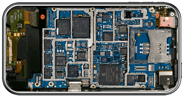
Impact of Ball Grid Array (BGA) Components
Ball Grid Array (BGA) components have a significant impact on PCB design and performance. These components offer many advantages, including improved thermal and electrical performance. They use solder balls arranged in a grid on the underside of the component, which helps in efficient heat dissipation and enhances the integrity of electrical connections.
Advantages of BGA Components:
- Improved Signal Integrity: The grid layout minimizes signal path lengths, reducing signal delay and enhancing performance.
- Better Thermal Management: The solder balls allow for more effective heat distribution, crucial for high-performance electronic products.
- Compact Design: BGAs allow for higher component density, essential for devices with limited space.
However, utilizing BGA components presents challenges in PCB design:
- Complex Manufacturing: BGAs require precise alignment during assembly, increasing the necessity for skilled technicians or advanced assembly technology.
- Repair Difficulty: Once soldered, it is often difficult to inspect and repair BGAs without specialized equipment.
When incorporating BGA components, PCB designers also need to consider special design requirements, such as ensuring proper alignment and accounting for the expansion of materials in different operating conditions. By leveraging these components efficiently, manufacturers can significantly improve product performance while managing production costs.
Mechanical Requirements in Stackup Design
In the design of a PCB stack-up, meeting mechanical requirements is crucial for ensuring product reliability and performance. The board’s thickness can affect the overall strength and thermal management. Typically, a thicker board is more robust, but it may increase production costs and affect flexibility.
Choosing the right layer count is vital. Common configurations include 4, 6, and 8 layer PCB stack-ups. More layers provide additional routing paths and better signal integrity but may affect the board’s mechanical properties.
Tables can be useful in comparing different stack-up configurations. For example:
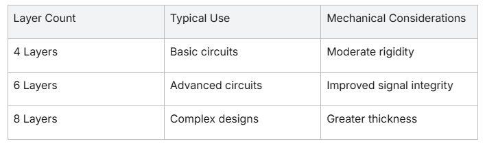
Using dielectric materials with suitable mechanical properties is essential. They must be able to withstand stresses during lamination.
Finally, ensure that the arrangement of copper layers is optimal. The outer and internal layers should balance between flexibility and strength. Proper design in these aspects leads to a durable, efficient, and cost-effective PCB.
Stackup Planning for Various Layer Counts
In PCB design, stackup planning is crucial. It determines how layers of copper and dielectric materials are arranged. This arrangement affects signal integrity, mechanical stability, and production costs. Different stacks suit different needs. Whether designing a simple circuit or a complex device, understanding the nuances of stackup planning can significantly improve a PCB’s performance and reliability. We’ll explore the considerations for 4, 6, 8, and 16-layer PCBs.
4-Layer PCB Stackup Considerations and Examples
A 4-layer PCB stack-up is a common choice in circuit board design, offering a balance between complexity, cost, and performance. The stack-up configuration impacts signal integrity, electromagnetic compatibility (EMC), and thermal management. Below, we outline key considerations and examples for designing a 4-layer PCB stack-up.
Key Considerations
Signal Integrity:
- Controlled Impedance: Ensure that impedance is controlled within acceptable tolerances (±10%) to maintain signal quality. This often requires careful selection of materials and precise layer arrangement.
- Signal Layer Arrangement: Typically, signal layers are placed on the top and bottom, with internal layers dedicated to power and ground. This minimizes crosstalk and enhances signal integrity.
EMC/EMI Performance:
- Ground and Power Planes: Place ground and power planes adjacent to each other to act as a reference plane and to reduce electromagnetic interference. This arrangement helps in suppressing electromagnetic radiation.
- Shielding: Use the ground plane as a shield for sensitive signal layers, reducing noise and protecting the circuit’s integrity.
Thermal Management:
- Heat Dissipation: Consider the thermal properties of materials to manage heat dissipation, especially in high-power applications. Use copper layers for better heat management.
Material Selection:
- Dielectric Thickness: Ensure a minimum dielectric thickness, such as 2.56 mil with two prepreg plies, especially for high-reliability applications complying with IPC class 3 standards.
- Material Properties: Choose laminates that align with the electrical, mechanical, and thermal requirements of the design.
Design for Manufacturability (DFM):
- Manufacturer Capabilities: Design the stack-up considering the capabilities of the PCB manufacturer to ensure the design can be accurately produced and passes DFM checks.
Example 4-Layer PCB Stack-Up
A typical 4-layer PCB stack-up might include the following layers:
Top Layer (Signal):
- Used for routing critical signals. This layer should be close to a ground plane to ensure low impedance paths for return currents.
Inner Layer 1 (Ground Plane):
- Acts as a reference plane for signals and provides a continuous path to reduce EMI.
Inner Layer 2 (Power Plane):
- Distributes power throughout the board and works in conjunction with the ground plane to provide low inductance power delivery.
Bottom Layer (Signal):
- Used for additional signal routing. Similar to the top layer, it should be paired with a ground or power plane to optimize signal integrity.
6-Layer PCB Stackup Considerations and Examples
When designing a 6-layer PCB stackup, several key considerations must be taken into account to optimize performance and ensure reliability. A well-planned stackup is crucial for minimizing electromagnetic interference (EMI), reducing signal crosstalk, and achieving the desired impedance, which are vital for high-speed and high-frequency applications.
Considerations for 6-Layer PCB Stackup
Layer Arrangement:
- A typical 6-layer stackup might include two outer signal layers, two internal power planes, and two internal ground planes. This arrangement aids in minimizing EMI and maintaining signal integrity.
Ground and Power Planes:
- Ensure there are dedicated ground and power planes. These planes provide a continuous return path for signals, reducing the loop area and minimizing EMI. They also help in reducing DC resistance and improving power distribution.
Trace Geometry:
- Carefully design trace width, spacing, and the overall geometry to achieve the desired impedance. This is crucial for maintaining signal integrity and reducing reflections.
Material Selection:
- For high-frequency applications, opt for materials with a low dielectric constant (Dk), such as Rogers or Isola. These materials help in maintaining signal speed and reducing losses.
Via Design:
- Use blind, buried, or stacked vias to connect different layers, minimizing parasitic inductance and capacitance. This is especially important for high-density interconnect (HDI) designs.
Signal Layer Isolation:
- Isolate high-speed signal layers from each other using ground or power planes. This helps in reducing crosstalk and improves overall signal integrity.
Flexibility:
- For rigid-flex designs, consider using polyimide materials for flexibility. This is particularly useful in applications where the board needs to conform to a specific shape or move during operation.
Examples of 6-Layer PCB Stackups
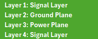
Standard 6-Layer Stackup:
- Layer 1: Top Signal Layer
- Layer 2: Ground Plane
- Layer 3: Inner Signal Layer 1
- Layer 4: Inner Signal Layer 2
- Layer 5: Power Plane
- Layer 6: Bottom Signal Layer
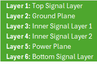
This configuration provides a good balance between signal integrity and manufacturing cost.
6-Layer Rigid-Flex Stackup:
- Layer 1: Top Rigid Signal Layer
- Layer 2: Rigid Ground Plane
- Layer 3: Flex Signal Layer
- Layer 4: Flex Signal Layer
- Layer 5: Rigid Power Plane
- Layer 6: Bottom Rigid Signal Layer
This setup is ideal for applications requiring a combination of rigid and flexible areas, such as in wearables or aerospace components.
High-Frequency 6-Layer Stackup:
- Layer 1: Top Signal Layer (Rogers Material)
- Layer 2: Ground Plane (Rogers Material)
- Layer 3: Inner Signal Layer 1
- Layer 4: Inner Signal Layer 2
- Layer 5: Power Plane (Rogers Material)
- Layer 6: Bottom Signal Layer (Rogers Material)
Utilizing Rogers material helps in maintaining performance at high frequencies, making this stackup suitable for RF and microwave applications.
In summary, a well-considered 6-layer PCB stackup can significantly enhance the performance and reliability of your circuit board, particularly for high-speed and complex applications. By carefully selecting materials, designing trace geometries, and arranging layers effectively, you can minimize potential issues related to EMI, crosstalk, and impedance mismatch.
8-Layer PCB Stackup Considerations and Examples
Creating an 8-layer PCB stackup requires careful considerations to ensure optimal performance, especially for high-speed applications. These stackups are increasingly used in complex designs where signal integrity, electromagnetic interference (EMI) control, and power distribution are critical. Here are some considerations and examples for developing an 8-layer PCB stackup:
Key Considerations for 8-Layer PCB Stackup
Signal Integrity and EMI Control:
- Signal Layer Placement: High-speed signal layers should be sandwiched between ground planes to create a stripline configuration, which helps reduce emissions and maintain signal integrity.
- Ground and Power Planes: Multiple ground planes are advantageous as they reduce ground impedance and help in EMI shielding. Power planes should be tightly coupled with ground planes to minimize noise.
- Return Path Management: Ensuring that every signal layer is adjacent to a ground plane allows for effective return path management, reducing inductance and potential crosstalk.
Material Selection:
- Choose materials with appropriate dielectric properties to support high-frequency signals. Consider the thermal and mechanical properties of these materials as well.
- Use software tools to aid in the selection of materials and to perform impedance calculations based on the stackup dimensions.
Symmetry and Mechanical Stability:
- Ensure that the stackup is symmetric to avoid mechanical stress and warping during fabrication.
- A cross-section implementation can provide further mechanical stability.
Layer Thickness and Spacing:
- Optimize the thickness of each layer to achieve the desired impedance. The spacing between signal layers and planes should be minimized to improve EMI performance.
- Use reinforced PTFE laminates or HDI processing if a thinner board is desired.
Power Distribution:
- Power planes can be partitioned into multiple large rails to support different voltage levels effectively.
- Coupling power planes with ground planes is crucial to reduce power noise.
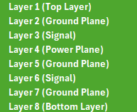
Example 8-Layer Stackup
Here’s a typical example of an 8-layer PCB stackup designed for high-speed applications:
Layer 1 (Top Layer): Signal layer for high-speed interfaces, often used for component placement.
Layer 2 (Ground Plane): Dedicated ground plane to provide a low-impedance path for signals on Layer 1.
Layer 3 (Signal): Internal signal layer for routing high-speed signals or control lines.
Layer 4 (Power Plane): Dedicated power plane, coupled with adjacent ground plane to minimize noise.
Layer 5 (Ground Plane): Ground plane for effective shielding and return path for signals on Layer 3.
Layer 6 (Signal): Additional internal signal layer, often used for medium-speed signals or control lines.
Layer 7 (Ground Plane): Another ground plane, providing additional shielding and return path for signals on Layer 6.
Layer 8 (Bottom Layer): Signal layer, often used for less critical routing and component placement.
Tailoring Stackups to Specific Applications
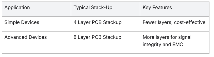
Designing a PCB stack-up involves tailoring it to fit specific applications. Each application has unique needs that affect the circuit board’s performance. For instance, a 4 layer PCB stackup is often used for simple electronic products, while an 8 layer PCB stackup suits more complex devices where signal integrity and electromagnetic compatibility are crucial.
Key Considerations in Tailoring PCB Stackups:
Layer Count: Choose based on the complexity and performance requirements. More layers offer better signal routing.
Signal Layers vs. Power and Ground Planes: Proper arrangement ensures optimal functionality and minimizes interference.
Dielectric Materials: These can affect operating frequency and thermal management.
Board Thickness and Copper Layers: Must meet design requirements for strength and conductivity.
Impedance Requirements: Layer arrangement affects signal integrity, especially in high-frequency applications.
Cost Considerations: More layers and complex designs can increase production costs.
Example:
By considering these factors, PCB designers can create optimized stack-ups that meet specific application needs.
Examples of Effective PCB Stackups
When designing a PCB, choosing the right stackup is crucial.
For a 4-layer PCB stackup, a common arrangement is:
- Signal Layer
- Ground Plane
- Power Plane
- Signal Layer
This configuration helps reduce electromagnetic interference and improves signal integrity.
A typical 6-layer PCB stackup could be:
- Signal Layer
- Ground Plane
- Signal Layer
- Power Plane
- Ground Plane
- Signal Layer
The extra ground plane helps with thermal management and further minimizes electromagnetic compatibility issues.
For an 8-layer PCB stackup, a simple setup might be:
- Signal Layer
- Ground Plane
- Signal Layer
- Power Plane
- Ground Plane
- Signal Layer
- Power Plane
- Signal Layer
This setup supports higher operating frequencies and complex circuits, making it ideal for advanced electronic products.
Using dielectric materials between layers maintains board thickness and optimizes impedance requirements.
PCB designers may use Altium Designer to visualize layer arrangements.
Considerations for layer count, mass production, and production costs are essential for meeting design requirements.
By strategically planning outer layers, internal layers, and copper layers, the production process ensures reliable performance.
Conclusion and Best Practices
A well-designed PCB stackup is vital for maintaining signal integrity and ensuring reliable electronic products. When planning your design, consider the layer count carefully. Whether it’s a 4, 6, or 8 layer PCB stackup, each choice affects impedance requirements, thermal management, and production costs.
Best Practices:
- Layer Arrangement: Use signal layers next to ground planes to minimize electromagnetic interference.
- Dielectric Materials: Select materials that meet electrical and thermal design requirements.
- Copper Layers: Balance copper layers to reduce warping during manufacturing.
- Impedance Control: Calculate impedance accurately, especially for high-speed circuits.
- Altium Designer Tools: Leverage software like Altium Designer for a clear view of stack-up configurations.
- Consult with PCB Manufacturers: Gain insights on board thickness and sequential lamination for cost-effective solutions.
- Flexible Materials: For mass production, especially involving flexible PCBs, verify the flexibility meets the product’s needs.
Adhering to these practices ensures signal integrity and reliable performance across various operating frequencies. Successful PCB stack-ups enhance the overall quality and efficiency of electronic products.
Frequently Asked Questions
In the world of electronics, PCB stackup configurations play a crucial role in determining the performance and reliability of circuit boards. Whether you’re a seasoned engineer or a beginner in PCB design, understanding these intricate details is vital. The arrangement and number of layers can significantly influence impedance, thermal management, and overall functionality of electronic products. This guide addresses common questions about PCB stackups, helping you make informed decisions for your designs.
What are the benefits of different stackup configurations?
Different stackup configurations offer varying advantages depending on the design needs. For instance, a 4 layer PCB stackup is often chosen for cost-effectiveness in simpler designs. It includes basic signal layers, a power plane, and ground planes, providing essential functionality without excessive expense. However, as complexity increases, a 6 or 8 layer stackup might be required. These bring added benefits such as improved signal integrity and electromagnetic compatibility, crucial for high-frequency applications. The additional layers can accommodate more intricate routing and better thermal management, essential for high-performance devices. Consulting with PCB designers and manufacturers can help determine the best configuration for specific impedance and design requirements.
How does layer count affect PCB performance?
Layer count is a pivotal aspect of PCB performance. More layers can offer enhanced signal routing options, contributing to better signal integrity. For instance, a circuit board with more than 4 layers can separate signal and power layers, reducing crosstalk and electromagnetic interference. Increasing the number of copper layers also allows for better control over impedance requirements, which is crucial for high-speed electronic products. However, more layers could increase production costs and board thickness. Consequently, the choice of layer count must be balanced between performance and budget considerations. It’s always wise to collaborate with a PCB manufacturer to optimize the layer stackup for efficient mass production.
What are common mistakes in PCB stackup design?
Designing a PCB stackup can be challenging, and several mistakes are common among designers. One frequent error is improper layer arrangement, such as not placing signal layers next to ground planes, which can lead to increased electromagnetic interference. Another common oversight is the selection of inappropriate dielectric materials, failing to meet the electrical and thermal design requirements. Additionally, designers might neglect impedance control, which is crucial for high-speed circuits. Overlooking thermal management can also lead to overheating issues. Lastly, neglecting to consult with PCB manufacturers could result in impractical design choices, affecting mass production and escalating costs. Awareness and careful planning can prevent these mistakes, ensuring reliable and efficient PCB performance.