QFN Socket
22/04/2025, hardwarebee
In today’s fast-paced electronics industry, miniaturization is the key to innovation, and the Quad Flat No-Lead (QFN) package is at the forefront of this trend. As devices become smaller and more efficient, understanding the intricacies of QFN packages becomes essential for engineers and designers alike. This package technology is favored for its minimal footprint, thermal efficiency, and cost-effectiveness, making it a crucial component in contemporary circuit design.
The QFN package, a prominent surface-mount technology, has a distinct structure characterized by its leadless design and efficient heat dissipation capabilities. It comes in various types, each tailored for specific applications, requiring precise footprint design and assembly to ensure optimal performance. Engineers must also be adept at solder joint inspection and rework techniques to maintain the reliability of these compact powerhouses.
In addition to comprehending the different types of QFN packages, choosing the right QFN socket is imperative. With numerous varieties of sockets available, each offering unique features, selecting the most suitable one for your project can be daunting. This article delves into the intricate world of QFN packages, covering everything from structural nuances to assembly tips, and guides you in choosing the perfect socket for your electronic needs.
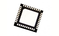
Overview of Quad Flat No-Lead (QFN) Package
The Quad Flat No-Lead (QFN) package is widely used in modern electronics. It is a type of surface-mounted technology used to house integrated circuits. Its design is crucial for enhancing electrical performance with an efficient heat path. This makes it a popular choice for various electronic devices. The QFN package provides a compact solution, aligning well with the industry’s push towards miniaturization. Its small package size and low-profile make it suitable for devices where space is at a premium. Package manufacturers are constantly looking to improve these attributes to meet growing demands.
Definition and Meaning of QFN
The term “Quad Flat No-Lead” describes a lead-free, flat package used in electronic circuits. It emerged as a reliable alternative to leaded packages like the ball grid array. QFN packages feature a flat design that supports stable ground and perimeter lands for electrical connections. They are especially valued for their role in minimizing solder joints and solder residues, reducing solder voiding. This results in better electrical performance and less stress from thermal expansion. In essence, QFN technology is essential for modern, efficient, and space-saving electronic designs.
Structure and Components of QFN
A QFN package consists of several key components that ensure its effective operation. The main body is a small, square flat package made typically from a copper alloy. Its structure supports an efficient heat path, allowing it to manage varying temperature ranges effectively. A ground pad at the center ensures stable grounding for electrical connections. The perimeter lands help form solid solder joints using a soldering process. This configuration contributes to the reduction of manufacturing costs by simplifying the assembly. The conductive adhesive used in joint formation ensures durable connections.
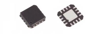
Types of QFN Packages
There are several types of QFN packages, each suited to different needs. Standard QFN packages are used for general applications and come in various sizes. Dual-row QFN variants offer increased connectivity, critical for high-performance electronics. Other package types include laminate-based QFNs, which provide additional flexibility. Each type supports specific requirements, such as efficient heat dissipation or accommodating greater pin counts. By choosing the right package size and type, device manufacturers can optimize for both performance and space efficiency. This versatility makes QFNs indispensable in the development of cutting-edge electronic devices.
QFN Footprint Design and Assembly
In the world of electronic devices, the design and assembly of quad flat no-lead (QFN) packages play a crucial role. These packages are known for their efficient heat path and smaller footprint. As technology advances, there is a greater need for compact, high-performance components. Manufacturers use QFN packaging to meet these demands, reducing overall package size while maintaining excellent electrical performance. This package type utilizes perimeter lands and a ground pad to ensure stable electrical connections. The design and assembly of QFN packages are pivotal for their smooth functioning and integration into various applications. Proper techniques ensure high-quality solder joints, minimizing issues such as solder residues or solder voiding.
Importance of Footprint Design
The design of a QFN footprint is essential for optimal electrical performance and manufacturing efficiency. An accurate footprint design enhances thermal management and supports the stable ground of the electronic components. Proper spacing of perimeter lands and the ground pad is critical to facilitate effective soldering and joint formation. Incorrect design can lead to issues such as increased manufacturing costs and poor temperature range management. It can also result in inefficient assembly, causing potential errors in solder joints. Considerations in footprint design include the copper alloy used for the pad, the conductive adhesive applied to ensure strong connections, and proper alignment. These elements work together to deliver optimal performance in integrated circuits.
Assembly Techniques for QFN
When assembling QFN packages, several techniques are crucial for ensuring reliable electrical connections. The assembly process begins with preparing the circuit board by applying solder paste to defined locations. The selection of solder paste impacts the soldering process, affecting joint strength and longevity. The placement of the QFN package must be precise to align perimeter lands with the solder paste. Reflow soldering is a widely used method due to its efficiency in forming durable solder joints. This technique carefully manages thermal expansion, mitigating defects during temperature changes. Optimized assembly techniques ensure strong joints, reducing the risk of failures in electronic devices.
Solder Joint Inspection and Rework
After assembly, it is important to inspect the solder joints to confirm their integrity and reliability. This inspection process helps identify any potential issues, such as solder residues or voiding, which might affect the performance of the QFN package. Tools for inspection can include microscopes and X-ray machines to examine joint quality. If any imperfections are detected, rework is necessary to maintain high-quality connections. Rework involves carefully removing faulty joints and reapplying solder with precision. This step is vital to avoid recurring problems and to ensure the overall durability of integrated circuits. By focusing on inspection and rework, manufacturers maintain high standards for electronic devices, reducing manufacturing costs associated with repairs and replacements.
QFN Package Socket Varieties
Quad Flat No-lead (QFN) package sockets are critical in connecting integrated circuits (ICs) to electronic devices. These sockets offer efficient electrical performance while keeping manufacturing costs low. Many package manufacturers create them due to their versatility and reliable electrical connections. Additionally, QFN sockets help improve heat dissipation, making them ideal for a wide temperature range. By using these sockets, engineers can maximize the performance of solder joints, which is essential in reducing solder residues and solder voiding. As technology advances, the demand for different package sizes and variants continues to grow, showcasing the importance of exploring various QFN package socket options.
Overview of QFN Sockets
QFN sockets are a type of flat package known for having a low-profile design. These sockets play a crucial role in ensuring stable ground connections and efficient heat paths for electronic circuits. Their popularity stems from their compatibility with different package variants like the ball grid array and other package types, such as leaded packages. Usually, made from copper alloy, these sockets ensure joint formation through perimeter lands. This reliable feature supports advanced electronic devices. The ability of QFN sockets to adapt to different single package designs makes them indispensable in the technology sector.
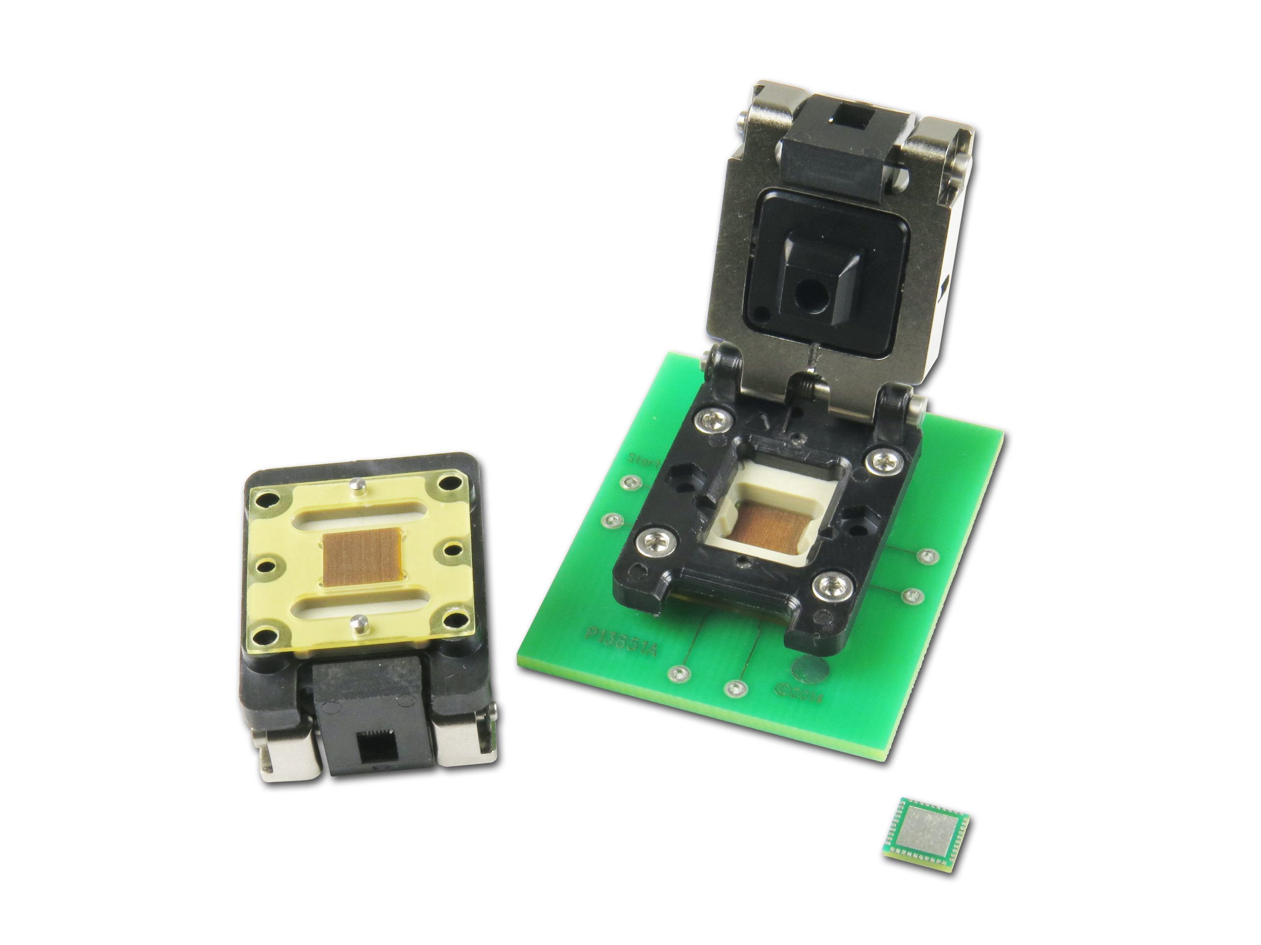
Source: Ironwood Electronics
Features of Sockets Types
The different types of QFN sockets each come with unique features suited to specific applications. Some common socket types include test sockets and burn-in sockets. Test sockets are often used during the initial testing phases of ICs. These sockets are designed for easy insertion and removal, allowing engineers to quickly assess the performance of chips. They utilize conductive adhesive and provide a stable environment for accurate testing.
On the other hand, burn-in sockets are meant for durability tests over extended periods. These sockets simulate prolonged use within a defined temperature range, crucial for determining an IC’s long-term reliability. They help identify potential failures due to thermal expansion and other stresses. Both socket types rely heavily on an efficient heat path to manage the generated heat in testing scenarios.
Manufacturers like Ironwood Electronics have developed innovative designs to address different needs. From minimizing manufacturing costs to enhancing electrical performance, they have tailored their products to suit various applications. Each socket type has its own attributes that enhance the soldering process, ensuring limited solder residues and reliable connections throughout the lifespan of electronic devices.
How to choose a QFN socket
Choosing the right quad flat no-lead (QFN) package socket is essential for optimal electrical performance. These sockets, used in electronic devices, support efficient heat paths and stable ground connections. Here’s how to select the ideal QFN socket:
- Package Size and Variants: Determine the size and variant of the QFN package. Look for options from reputable package manufacturers that suit your specific integrated circuits.
- Electrical Connections: Ensure robust and reliable electrical connections. Check for perimeter lands, stable ground pads, and an efficient heat path to manage thermal expansion.
- Soldering Process: Consider sockets that optimize solder joints and minimize solder voiding. An ideal socket should manage solder residues and ensure solid joint formation.
- Material: Opt for sockets made from copper alloy for durability and long-lasting electrical performance.
- Cost and Compatibility: Evaluate the manufacturing costs and ensure compatibility with your ball grid array and leaded package needs.
- Temperature Range: Confirm that the socket supports the required temperature range for your application.
Choosing the right QFN socket involves balancing these factors to ensure efficient performance and reduce long-term costs.
Conclusions on QFN Package Sockets
Quad flat no-lead (QFN) package sockets play a crucial role in modern electronics. Their low profile and efficient heat path make them ideal for integrated circuits. QFN packages offer excellent electrical performance and reliability compared to traditional leaded packages.
Benefits of QFN Package Sockets:
- Efficient Heat Dissipation: Copper alloy in QFN packages provides an efficient heat path, reducing thermal expansion and enhancing performance.
- Size Variability: Available in various package sizes, QFN sockets offer flexibility for different electronic devices.
- Improved Electrical Connections: The design eliminates lead forming, leading to better electrical connections and reduced manufacturing costs.
In conclusion, QFN package sockets are preferred for their superior thermal and electrical properties. Their ability to minimize solder voiding and facilitate strong joint formation improves reliability. Manufacturers like Ironwood Electronics provide various QFN package variants, offering solutions for different temperature ranges and applications. QFN sockets ensure stable ground and perimeter lands for advanced performance in single package designs.