The Ultimate Guide to Chip Antenna
10/04/2024, hardwarebee
Introduction
The drive for size miniaturization in wireless electronics devices led to antennas being reduced in size and deployed in an ultra-compact way, which is referred to as chip antenna technology. New antenna designers are always coming up with novel techniques to minimize size, save costs, and enhance the performance and efficiency of the antenna. The compactness of chip antennas makes them an appealing alternative for smaller integrated applications.
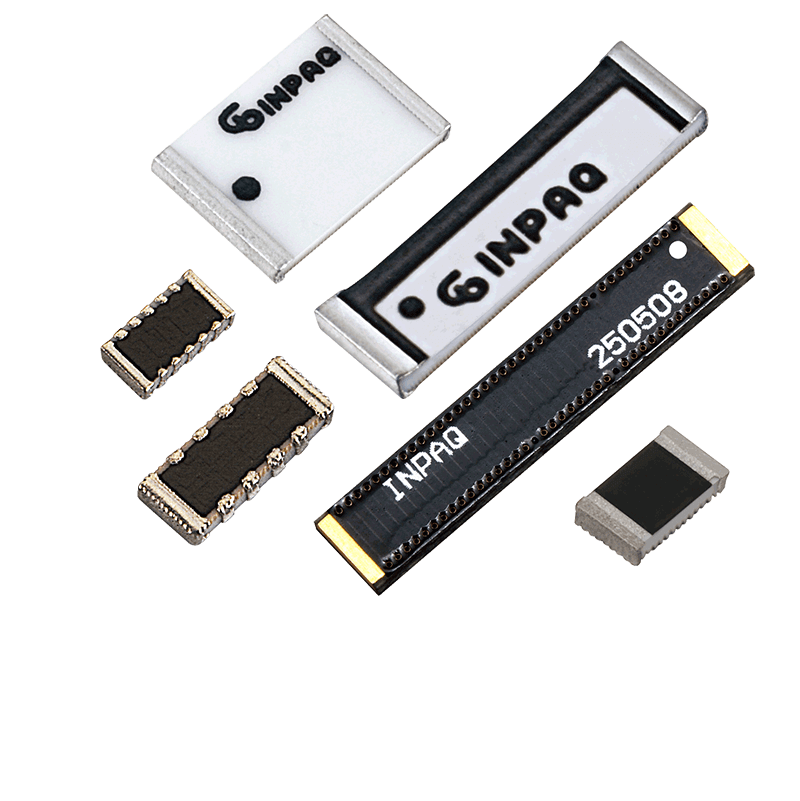
Definition of Chip Antenna
Chip antennas are very small, ultra-compact, and low profile antennas that are fabricated directly onto silicon chips or ceramic substrates. Such antennas are commonly used in space-limited wireless devices like smartphones, tablets, and laptops.
Overview of Chip Antenna
Chip antennas, being very small antenna elements, may be readily mounted in electronics circuit elements that are typically a few millimeters square. Their ultra-compact size makes them well-matched for many space limited applications including Bluetooth devices, RFID tags, and mobile devices. They can be conveniently positioned next to any electronic components on the circuit boards, empowering more improved PCB layouts and integrations of the antenna into devices. Even certain chip antennas are slightly flexible and can be molded directly onto devices for further improving integrations. Microstrip patch antennas, Inverted-F antennas, meandered antennas, and fractal antennas are the most used antenna types that can be easily integrated into chips due to their low profile behaviors.
Importance and application of chip antenna for Modern Electronics
Owning to the ultra-compact size and the capabilities of integration into smaller and portable gadgets properties, chip antennas play a crucial role in enabling seamless connectivity in modern electronics. Modern electronic devices demanded to be smaller, portable, wearable, and connected. The only option that enables wireless connectivity at this microscopic size, easily embedded in the system without affecting the desired dimension is a chip antenna. Currently, chip antennas are used in a wide range of applications such as wearable devices, portable products, IoT systems, automotive electronics, and medical electronics, by reducing the size and creating connectivity to establish a wireless data transmission for various applications such as navigation, monitoring, etc.
Advantage and Disadvantage of Chip Antenna
Chip antennas are more prominent in their ultra-compact size advantages, which enable easy integration for space limited electronics components. In addition, a single-chip antenna also supports multiple wireless standards like Bluetooth, Wi-Fi, and GPS, it shows that the antenna is cost and space effective. Furthermore, the antenna is simple for manufacturing and easy for optimization, it can be directly mounted on the PCB or molded indeed the devices.
Even though chip antennas have the above mentioned advantages, they have many disadvantages when compared to other traditional antennas. The most common disadvantage of using chip antennas is they have a low performance which is directly related to the size reduction of the antenna, they operate with narrow bandwidth, and are poor efficient. The other bottleneck in chip antenna technology is their radiation is highly influenced by the device geometry and nearby metallic components or ground plane size. As a result, the radiation characteristics of the chip antenna are always re-assessed for any device change, if the geometry and components are changed.
Types of Chip Antenna
Chip antennas are classified into several varieties based on the materials used for their productions. Each antenna has unique appealing qualities and benefits over the others, thus they may be chosen differently in the application.
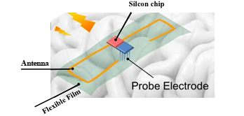
Silicon Chip Antenna: Its manufacturing employs a photolithography technology that is fabricated directly on the silicon or other semiconductor devices in the circuit to enable a high miniaturization of the antenna. The most common antenna designs seen in semiconductor devices are planer Inverted-F antennas, patches, and spiral designs. Silicon chip antennas may be integrated with any RF components like amplifiers, filters, or switches for compact transceivers. These antennas suffer a conduction loss at mm-wave and microwave frequencies. Figure 1 shows an example of such an antenna in a 2 mm x 0.3 mm Inverted-F antenna type for implantable medical applications.
Figure 1: Example of silicon based chip antenna
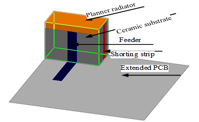
Ceramic chip Antenna: It is constructed by the low-temperature co-fired ceramics (LTCC) technology on ceramic materials such as zirconia, which are heated at high temperatures in small sizes. The ceramic substrate provides a greater dielectric constant than the PCB material, allowing for thickness reduction and low dielectric losses at high frequencies. Ceramic materials have an excellent resistance to environmental factors like moisture and chemicals. These chip antennas are commonly used in applications that need ruggedness like automotive telemetric units, industrial IoT, and embedded sensors. Figure 2 illustrates a planer type ceramic chip antenna structure on a PCB.
Figure 2: A Ceramic planner chip antenna
PCB Trace Chip Antenna: These chip antenna types are manufactured by etching conductive traces directly on the PCB surface. The radiating elements of the antennas are possibly designed as a monopole, dipole, Inverted-F, loop as a trace with a simple way of integration. As a PCB antenna, this type of chip antenna performance has a direct relation to the PCB thickness, dielectric constant, and proximity to other components. It is a little susceptible to damage during assembly unlike ceramic or flexible chip antenna. They have low efficiency, poor ruggedness, and limited frequency range. Figure 3 shows an example of a PCB Trace printed monopole antenna.
Figure 3: Example of PCB Trace printed monopole chip antenna
Flexible chip antenna: Such chip antenna types are printed on flexible dielectric substrates like polyimide films and liquid crystal polymer (LCP). It makes them wrap around the curve or flexible integration for products like wearable, as shown in Figure 4. The types of antennas like folded dipole, monopole, and planner Inverted–F antennas are commonly used in polyimide with a thickness of 50-100μm. They can be used for drone or aerospace applications due to their weight. Their demand is growing in wearable devices, 5G phased array, IoT tags.
Figure 4: Example of flexible wearable printed folded dipole antenna
Comparative Analysis
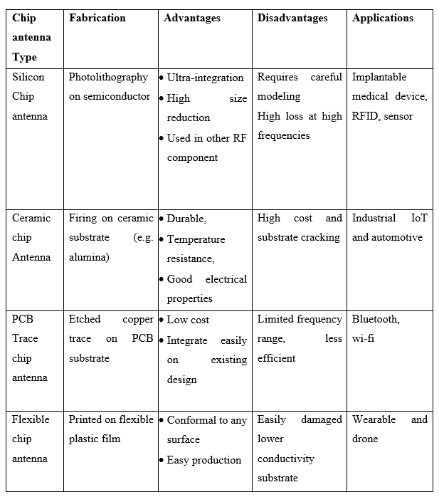
The following table will summary the different types of chip antennas in terms of application area, fabrication, and advantages and drawbacks.
Table 1 Comparison of various types of chip antenna
Design Consideration for Chips Antenna
To design a chip antenna, the designer must consider several variables. For instance, the antenna types, dimensions, and geometries must be selected to resonate at the required operating frequency while fitting into the chip size. The radiation properties of the chip antenna are strongly influenced by the conducting materials, substrate materials, and the size of the ground plane. In addition, the power handling capabilities of the chip antenna need consideration. Furthermore, the designer must repeatedly examine the desired performance parameter of the antenna. Integration issues like interference, fabrication constraints, and environmental factors must be taken into account.
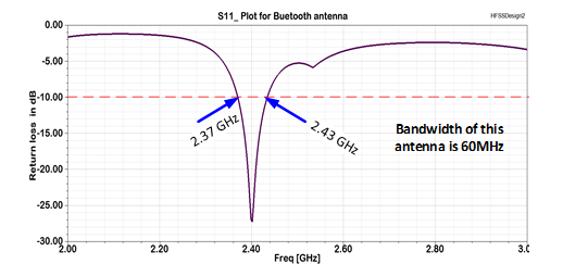
Another important factor that affects our design is the matching network, the feedline of the antenna must match the antenna for maximum power transfer. The antenna can have a separately designed network to eliminate mismatched loss. When the chip antenna is well-matched the return loss will dipper to negative infinity dB (commonly s11 <-10dB), as shown in Figure 5. That means maximum power transfer between the antenna and transmission line is verified at the operating frequency.
Figure 5: Return loss of a chip antenna for Bluetooth applications with 60 MHz band
Factors Influencing the Performance of Chip Antennas
There are a number of factors that reduces the performances of chip antennas. The first factor is the size of chip, which is significantly less than the operating wavelength of the antenna, rendering the antenna inefficient and degrades its performance. The size, geometry and proximity of ground plane/metallic devices have an impact on the performance of chip antenna by producing a mismatching. Furthermore, the chip antennas bandwidth and efficiency affected by the thickness, dielectric material and loss tangent of substrate. The positioning of antenna on the chip is another element that influence the performances. Thus, chip antenna performance must revalidate if the layout is changed. On the other hand, external factors like environmental conditions, obstructions, nearby electronics components, accuracy of etching, or printing physical dimensions, signal reflections through multipath fading are considered as additional factor.
Techniques for Optimizing Chip Antenna Performance
Engineers and researchers of chips antennas are always striving to optimize and modify the chip antenna by employing different techniques to minimize the hindrance factors and boosting the level of performance. From their techniques this paper summarizes the following
- Adjust the shape, widths, lengths and number of radiating element inside the chip.
- Proper selection of lower loss, good electrical properties substrate material that matches the desired application
- Design appropriate impedance matching network
- Use varieties of techniques like slot, EBG strategies, reconfigurability, adding reflector or director parasitic, and multi staking for performance optimization.
- Simulate with full wave EM simulator and apply high-tech prototyping techniques for testing like 3D printing.
Integration of Chip Antenna in PCB Designs
For many electronics components, chip antennas are well-suited on PCB designs, however, their integration requires various considerations such as the PCB layout design, placements, orientations, proximity with others and the enclosure materials.
PCB Layout Design and Antenna Placement Considerations
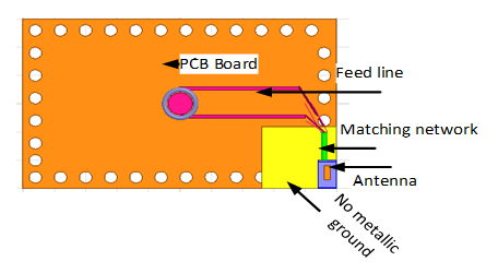
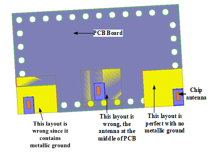
The first crucial stage in integrating chip antennas into PCBs is to design the PCB layout and enclosure materials. PCB components get increasingly dense as their sizes shrink, and chip antennas are extremely sensitive to power and ground plane size. The radiation properties of chip antennas require appropriate ground plane size. For the chip antenna, the PCB itself acts as the ground plane, the antenna is required to be placed on the top of the edge of the PCB. The position must be free from ground and metallic components that will degrade the performance of the antenna. Figure 6 illustrates the proper placement and not-proper positions of the chip antenna on the PCB.
Figure 6: Chip antenna positions on PCB layout design.
Techniques minimizing interferences and maximizing efficiency
In addition to the proper placement of chip antenna on the PCB and providing sufficient ground plane for good radiation. Techniques that enhances the performance of chip antennas by reducing the interferences. It includes removing any conductive plane under the chip antenna will avoid absorption of radiation. In addition, apply filtering, impedance matching as well as decoupling to reduce the interferences from other electrical components. Removing or minimizing encasing the chip antenna from a metallic enclosure is also one of the methods for efficient radiation. If the metallic enclosure is applied, the antenna’s radiation is reflected without transmission. The most common antenna housing types are polymers to protect the chip from harsh environmental factors.
Testing and Validation of Chip Antenna
Measuring and testing the antenna is critical for the performance evaluation of the chip antenna before producing the final product. Validation can be done through the different chip antenna parameters.
Testing Techniques of Chip Antenna
Gain measurements: It compares the radiated signal strength to the isotropic radiator. The commonly used gain measurement method is substitution techniques which is also called the gain transfer method, it requires a reference antenna with deterministic and reliable gain characteristics.
Reflection coefficient (S11) measurements: It determines how the antenna is well-matched with the feeding circuit and it can be measured using Vector Network Analyzer (VNA). When the test setup is calibrated for reflection coefficient measurements using an Impedance Standard Substrate (ISS). It uses a reference transmission line impedance of 50 Ohms. Finally, the observed findings are compared with simulated results.
Radiation Pattern Measurements: It will assist the designer by testing the level of radiated power and direction of the radio signal over the 3D space. This measurement can be used by using an antenna positioner/ scanner and anechoic chamber. The chip antenna is placed in the middle of the reference antenna and then the antenna spins in θ and φ over the sphere surrounding the test distance. The results are recorded with the directivity pattern of the chip antenna at the operated frequency.
Finally, the measured results are compared to the simulation results to determine whether the chip antenna meets the intended criteria. Analyze the measured parameters to validate the antenna against the parameter checklists.
Importance of Compliances and Certification
The finished product of the chip antenna must be examined in conformity with regulatory organizations. This evaluation comprises a frequency of operation, radiating power, materials property, and others with respect to the guideline on their policy. It is essential to have such a test and certification before mass production, commercialized, and public use of the chip antenna product.
Practical Applications of Chip Antenna
Practically, chip antennas are integrated into modern electronic devices to transmit or receive electromagnetic signals wirelessly. Among them, item tracking or access control is one practical application of chip antennas by integrating them with RFID tags. They are also used in creating as they are embedded easily in many electronics like Wi-Fi routers, Bluetooth devices, mobile devices, and other modems. In addition, developing smart agriculture and supply chain tracking also other practical applications of chip antennas by integrating them with IoT sensors. The application of chip antennas also extended to structural healthcare and automotive industries. They can assist general healthcare applications when they are integrated into medical equipment. They are also applicable in the automotive industry just like collision avoidance radar systems, keyless entry systems, and tire pressure monitoring applications.
Challenges and Future Trends in Chip Antenna Technology
Chip antennas have various applications and excellent features in antenna technology but they face several integrations, manufacturing, and practical obstacles. However, several technological development and optimization techniques are adopted for future utilization of chip antenna.
Current Challenges in Chip Antenna Design and Integration
Maintaining the radiation properties of chip antennas with further size reduction and the market demand for smaller devices is a big challenge in chip antenna technology. When the antenna size is miniaturized and device densities are raised, the antenna becomes mismatched, less efficient, and has a significant near-field coupling impact. However, most modern electronics demand smaller sizes, multi-functionality, and high data rates. Thus, chip antenna designers are facing a great challenge while trying to attain a multiband and wideband operation. There are also other challenges like size, compatibility with other materials, packaging stress, production efficiency, excessive heat dissipation, and so on.
Emerging Trends and Innovations in chip Antenna Technology
Some of the challenges in chip antenna may be solved by the emerging trends and innovations in chip antenna technology. For example, the development of RF switches allows the chip antennas in pattern and frequency reconfigurability. The mechanical compatibility and robustness issues are also solved by the multilayer 3D printing technology and 2D materials. The development of automated design processes through AI technologies to reduce iteration and complexity in designing chip antennas. The mm-wave technologies allow multiple smaller antenna integration using the system-in-package mechanism for diverse applications. The other important innovations for chip antenna technology are RF energy harvesting techniques and combining multiple arrays for high directive using adaptive beamforming techniques. The existence of a co-designed thermal management system for chip antenna is assisted in reducing damage due to extensive heat dissipation.
Predictions for the Future of Chip Antennas and their Applications
With the introduction of the aforementioned revolutionary technologies in chip antennas, their future applications will include wireless ubiquitous connection with high data rate services, particularly for mm-wave and terahertz applications. As demand for smaller-sized devices grows, so does the chip antenna. It is essential to the development of smaller and more efficient wireless devices
Real Examples of chip Antenna Devices
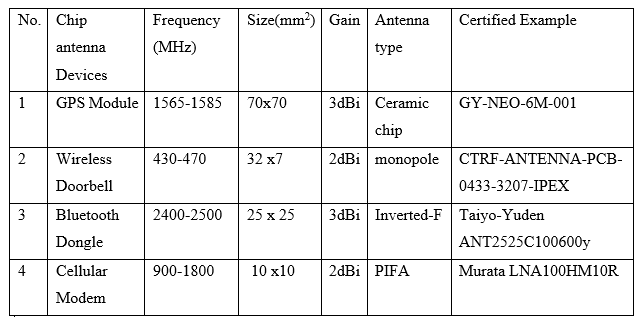
The following applications are real examples of modern chip antenna technologies. The comparison of them in terms of gain and size, operating frequencies, antenna types, and example of certified antenna are shown in Table 2.
Table 2 Comparison of different real chip antenna examples with their applications
Chip Antenna Companies
Here is a list of 5 chip antenna companies and their websites:
Abracon – Website: abracon.com
Abracon is a leading manufacturer of precision electronic components, including chip antennas. They offer a wide range of standard catalog products and also develop custom chip antennas upon request.
Frontier Electronics Corp. – Website: frontierusa.com
Frontier Electronics Corp. is a manufacturer of passive components, including chip antennas. They specialize in diodes, MLCC capacitors, and magnetics such as air coils and transformers.
RFMW – Website: rfmw.com
RFMW is a supplier and distributor of specialized radio frequency (RF) and microwave components. They offer a range of chip antennas, along with other RF and microwave components.
Johnson Electric – Website: johnsonelectric.com
Johnson Electric is a manufacturer of motors, micro-switches, solenoids, microelectronics, and flexible printed circuits. They also offer chip antennas for various applications.
TE Connectivity Ltd. – Website: te.com
TE Connectivity is a designer and manufacturer of sensor and connectivity solutions. They offer chip antennas as part of their product portfolio for applications in various industries.

