Ultimate Guide: Linear Voltage Regulators
19/07/2021, hardwarebee
Power supply is one of the most fundamental blocks of any electronic product. However, this stage is often overlooked by designers, even experienced engineers, due to the misleading assumption that a supply voltage is always constant, stable, and ideal. Electrical power can be directly obtained from batteries, local energy sources (solar panels, mechanical absorbers, fuel), and the electric power system. Independent from the source, this voltage must be adjusted and stabilized before powering our electronic devices. Moreover, different electronic devices may use different voltage levels (3.3 V, 5 V, 9 V), so the supply voltage must be adjusted in several regions of the circuit. Finally, electronic circuits have a finite PSRR (Power Supply Rejection Ratio), so any noise and stability coming from the source may be injected into the signal chain.
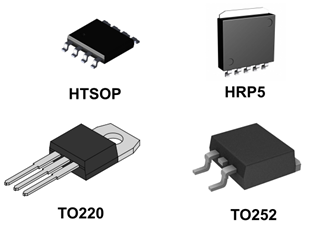
Figure 1: Typical Linear Voltage Regulator Packages
Voltage regulation can be implemented using linear regulators and switching-mode voltage regulators. Switching-mode voltage regulators are voltage converters (step-down and step-up) that uses switches to control the delivery of power to the load, and this control can be designed to set the output voltage to a specific level, independent on the input. Switching-mode voltage regulators usually implement MOSFET switches combined with capacitors and inductors to perform the power delivery. Linear voltage regulators, on the other hand, do not use switches on its application. Instead, rely on the intrinsic behavior of the components involved (transistors, diodes, operational amplifiers, resistors) to adjust and stabilize the voltage. In this tutorial, we are going to discuss linear voltage regulators.
The Voltage Divider
Before we can understand how the practical voltage regulator works and why it is designed as it is, we need to discuss the simplest form of voltage adjustments and its limitations. The basic voltage divider is composed by two resistors and, optionally, an output buffer, as seen in the figure below.
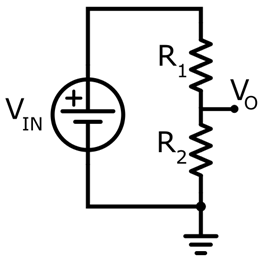
Figure 2: Voltage Divider
The voltage drop caused by the divider reduces the initial voltage, so this is a step-down regulator. The output voltage can be calculated as:

Let us say that we have a 5V source, and we need to feed a 3. V integrated circuit. If R2 = 50 kΩ, R1 should be equal to 25.76 kΩ. Although this circuit provides the voltage adjustment, it fails to give ideal source properties due to the large resistor values. And if we design it using small resistors, the power consumption rises absurdly. Output buffers using operational amplifiers or transistors, as seen in Figure 2, can be used to eliminate this problem. However, the voltage is not regulated: if the input rises to 6V during a power surge, the output will rise to 3.96 V, and we may damage our IC. Therefore, although simple and straightforward, the voltage divider is not a good approach to adjust the voltage supply level.
Diode Regulation
Different from voltage dividers, forward biased diodes can keep its voltage drop almost independent of the current and of the input voltage. So if we add a forward biased diode in parallel with R2 in Figure 2, the output voltage VO should be independent on the input. However, the output voltage will be equal to VD, that is typically VD = 0.7V. Thus, the circuit is not flexible, and several diodes in series should be used to obtain higher voltages (for example, five series diodes are needed to obtain 5V). To solve this issue, Zener diodes can be used, as shown in Figure 3.
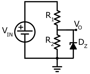
Figure 3: Zener Diode as a Voltage Regulator
Zener diodes can be biased reversely to obtain higher voltages. Zener diodes with VZ = 3.3V, 2.5V and 4.7V are common in the market, so these voltages can be directly obtained using the circuit. However, this approach has several limitations:
- Low efficiency for heavy load currents due to the series resistor
- Zener impedance is not zero
- Values are limited to the Zener voltage
- Voltage varies with temperature
Linear Voltage Regulator
In order to obtain regulated and stable voltage, a linear voltage regulator circuit must be immune to variations and noise coming from the input. Also, it should be able to maintain the supply voltage constant for any level of power consumption. That is, the current drawn by the circuit cannot change the voltage value significantly. To fulfill these requirements, the voltage regulator must attend some basic characteristics:
- Low output impedance
- Immunity to environment (temperature, humidity, noise)
- Immunity to input voltage variations, surges, and noise
- Enough current driving capability (depends on the application)
The linear voltage regulator is a three terminal device designed to fulfill the abovementioned requirements. The device (Figure 4) is composed by the input voltage pin, the output voltage pin and a ground connection. The linear voltage regulator is a very powerful tool in electronics, and is the standard in low power supply management systems, especially in local voltage conversion in the PCB.
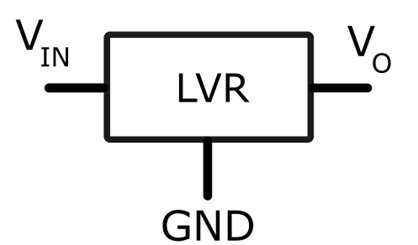
Figure 4: Linear Voltage Regulator
Compared to switching-mode regulators, linear regulators are able to provide lower noise and complexity, at cost of being more inefficient than their switching counterparts. The voltages available range from 1 to 24V, and are capable to drive currents as high as 5A.
The working mechanisms of a linear voltage regulator is based on both voltage divider and Zener regulator circuits. Figure 5 shows a generic block diagram of a typical linear regulator. The three-terminal device showed in Figure 4 is a representation of the integrated circuit. The output voltage is defined by a voltage reference stage, that can be implemented using bandgap references, which are independent of temperature. This voltage reference is compared with the output using a voltage divider and an error amplifier, and the negative feedback of the whole circuit reduces the output error to zero. The stage called “pass device” is responsible for adjusting the voltage drop according to the error voltage, thus regulating the supply.
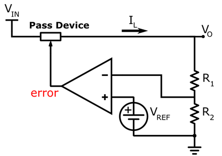
Figure 5: Linear Voltage Regulator Block Diagram
The output voltage can be calculated as follows:

However, when selecting a voltage regulator for your design, this equation is irrelevant, as all elements of Figure 5 are inside the integrated circuit, and the output voltage is defined by the manufacturer. The implementation of the block diagram varies from technology to technology, but typically all stages are designed to provide stable and low power dissipation. However, because of the intrinsic voltage drop across the pass device, linear voltage regulators are not very efficient. The equation below describes the power dissipation of a typical voltage regulator:

Notice that the current is dependent on the load, and the voltage drop depends on the application. Therefore, this term cannot be optimized by design, which causes the efficiency limitations inherent of linear voltage regulators. Nonetheless, the minimum voltage drop allowed through the pass device is usually optimized in design. The term represents the losses from the other stages.
Besides the fundamental features that composes the linear voltage regulator, some extra peripherals are typically included in commercial voltage regulators. Shutdown control allows the user to disable the circuit, saturation sensor provides information about internal overloads, temperature sensors can control the output to avoid overheat, and a current limiting stage.
How to Select a Linear Voltage Regulator
Although the internal design of integrated voltage regulators is important, it is not really relevant for system designers that want to simply apply this circuit in their circuits. Therefore, this section will present a quick guide on how to select the voltage regulator that best fits your design. Before scrolling through lists of different models and manufacturers, first you need to identify the following design specifications:
- Input Voltage and Output Voltage: the input voltage is defined by the supply voltage to be regulated, and the output voltage is the regulated supply level that is required by your device. Sometimes, the circuit needs multiple regulators: for instance, embedded systems may require a 3.3V regulator to feed the microcontroller and 5V or 12V regulators to supply sensors and actuators.
- Dropout Voltage: some systems require a small drop in voltage between the source and the output. For instance, your system may need to get 8 V from a 9 V source, so the required dropout is 1V. Furthermore, some supply sources, such as batteries, suffers from voltage reduction over time, and using a low dropout voltage regulator may increase the autonomy of your device.
- Power Draw: one of the most fundamental specifications is the amount of power needed. If your device draws more current than the regulator can supply, the output voltage will drop, and the regulator can even be damaged. Therefore, the model specification must comply with your power requirements. If your power demand is too high, consider using switching regulators instead.
- Noise: electronic circuits are not completely immune to supply noise, and critical applications (such as electronic instrumentation) may require very “quiet” regulators. In these cases, the regulator noise must be considered in the selection stage of the design.
Circuit Design Consideration
Bypass Capacitors
Linear regulators are very simple circuits, but to extract the most out of this component, one should be careful when designing the power stage, especially the PCB. Firstly, linear regulators have limited frequency response, and to apply them to fast signal circuits, one should use bypass capacitors. The bypass capacitors are able to provide the low impedance path for fast currents without affecting the regulator behavior. However, because the regulator is a feedback circuit and sometimes sensitive to output capacitance, the capacitor specifications must be within the recommended range of the datasheet, to avoid instability.
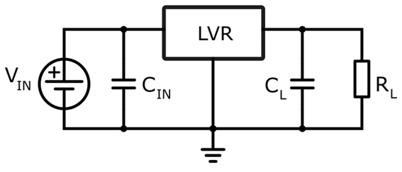
Figure 6: Linear Voltage Regulator with Input and Output Capacitors
Thermal Considerations
Linear regulators are power providers. Therefore, temperature must be considered to keep the circuit in the optimal operation range. High temperatures can change the output voltage, decrease efficiency, and even damage your device. To avoid these issues, temperature dissipation must be provided in some cases. The first step in this case is to identify the dissipated voltage, which can be roughly estimated using the equation:

This equation is simplified, only considering the dissipation caused by the voltage drop, which is enough in most cases. After finding , the datasheet should be consulted to check if the is below the recommended values at the desired temperature. If not, thermal dissipation should be applied. Usually, the manufacturer provides thermal design guidelines, but the designer can also use the thermal resistance of the device to calculate how much dissipation is needed to keep the junction temperature at the recommended temperature.
PCB Design Guidelines
Finally, the PCB design must be optimized. This step is constantly overlooked, but the power section of your circuit can be significantly improved by following some simple design rules:
- The regulator should be placed as close as possible to the circuit they are feeding, to avoid noise pick-up and line resistance.
- Bypass capacitors should be placed near the supply pins of each integrated circuit fed by the regulator.
- The width of power traces can be used to reduce heat from the regulator. Therefore, using large copper traces can increase the thermal dissipation.
- Some packages offer a thermal pad. Usually, this pad is connected to ground, and it should be directly connected to large ground traces or to ground planes (using vias) to minimize thermal resistance.
- Heat dissipating traces should be left without solder mask, to keep a direct contact between metal and air.


