
The Ultimate Guide to PCB Manufacturing Process
30/04/2019, hardwarebee
If you were to disassemble an electronic product and take a peek inside, you will very often find a plate or a board with numerous components stuck onto it — this is the PCB and it is basically the glue that connects all the different components together and makes them operate.
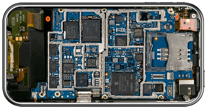
PCB stands for a Printed Circuit Board and is essentially a piece of board that consists of printed wires that provide electrical connectivity for all the components assembled on the PCB.
The way that a PCB is able to conduct electricity is by a series of copper wires that have been meticulously placed on its surface. The pattern of these wires is what ultimately determine how the product works and the purpose it serves. You can image those wires to be like streets that connect different house.
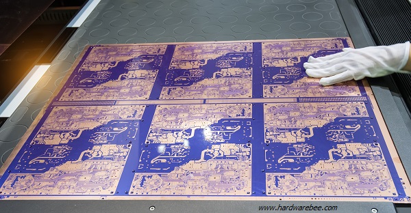
So even though they may look harmless and inconspicuous and not all that difficult to create considering it’s just a board with a few circuits on it, it is a critical component that actually undergoes quite an elaborate manufacturing process.
Let’s take an overarching look at the manufacturing process that results in the production of a PCB and how each step contributes to its creation.
PCB Manufacturing Process
Step 1: the design
The process of any manufacturing practice begins with the development of a basic design. A detailed blueprint of the circuit board must have been created beforehand.
Step 2: the print
The PCB is printed using a plotted printer which produces a resultant film that shows the various layers and intricacies of the circuit board. The black ink will represent the conductive copper pathways and circuits while the clear ink represents the non conductive areas. This is applicable to the inner layers. When we reach the outer layers, this representation is reversed.
Step 3: the substrate
The substrate is made up of insulating material, namely epoxy resin and glass fiber. The purpose of the substrate is to connect all of the various elements. The materials are semi cured in an oven and then the design of the board is etched onto it.
Step 4: the layers
A laminate is created of the inner layers using the blueprints. Covering this laminate is a photosensitive film called the resist which will harden under Ultraviolet light, helping in the alignment and the printing of the circuit board along with drilled holes.
Step 5: the bonding
The panels are then sent to a room where they are exposed to beams of Ultraviolet light in order to harden the photoresist layer. This actually reveals the underlying copper pathways and connections.
Step 6: the refining
An alkaline chemical solution is used to remove any unwanted copper from the board without causing any harm to the photoresist layer.
Step 7: the inspection
The layers are inspected by automated machines to ensure that everything is aligned and in place.
Step 8: the lamination, pressing, and drilling
All of the layers are now pressed together and laminated as they are held in place with clamps using an epoxy resin called prepreg. Over the prepreg is a layer of substrate and copper foil, topped o with more resin and another copper layer. A mechanical press then presses everything together and punches pins through them to keep them in place. Heat and pressure are applied to melt the epoxy and cause the layers to fuse. Lastly, a computer guided grill is used to drill on various holes through the layers so as to expose the substrate as well as the inner panels.
Step 9: the plating
The panels are first thoroughly cleaned and then are bathed in a series of chemicals which deposits a thin layer of copper on the surface of the board. This coper covers the plate and enters the walls of the holes.
Step 10: the outer layer imaging
Like one of the steps mentioned before, we apply a photoresist again while imaging the outer layers of the design and then harden it using Ultraviolet light. The panel then goes through a machine that removes the unwanted and unhardened photoresist, ultimately resulting in a product that is basically an inversion of the inner layers of the PCB design.
Step 11: the plating
Using electroplating techniques, a thin layer of copper is applied to the board and the exposed areas take up the material. After that, the board undergoes tin plating which protects the underlying copper pathways that are meant to form the various path and connections of the circuit.
Step 12: the final etch
In this step, the tin serves to protect the copper material that is required on the board from being removed while the other bits and pieces that remain exposed and unprotected are removed using a chemical. This establishes the conducting areas, connections, and pathways.
Step 13: the application of the solder mask
This is the point where the board is ready for a coat of solder mask. It is important to ensure that the panels are clean before this layer is applied. This is essentially an epoxy solder mask in that is later solidified using Ultraviolet light through a solder mask photo film. This actually gives the board its characteristic green color.
Step 14: the surface finish
A surface finish is the last solderable coat which will help improve the bonding of the elements to the board and increase the quality of the adhesion, this finish can be achieved using a number of different materials, including silver and gold.
Step 15: the silkscreen
As it nears completion, the printed board is silkscreened using an inkjet which actually prints out the critical information associated with the board onto it as a last coat.
Step 16: the final test
An electrical test is run on the newly synthesized circuit board in order to ensure that it is in working order and offers the functionality it is supposed to. This may either be performed by a practiced technician or in an automated manner in a controlled environment. The testing pattern depends on the original designs of the board.
Step 17: the cutting
Finally, once the designing, execution, and testing is complete, the manufacturing of the PCB is brought to a close by a machine cutting out a number of boards from an original panel using a router or a v groove, with the former leave tabs on the edges of the cut out board for extraction and the latter cutting diagonal channels on either sides of the board.


