
FPGA Tutorial
26/06/2021, hardwarebee
Field Programmable Gate Arrays (FPGAs) are the the most efficient, cost-effective and reconfigurable solution for the hardware applications. It consists of re-programmable blocks which helps a user to reprogram for any given application.
The purpose of this tutorial is to focus on the FPGA design process and tools which are required to program an FPGA, in addition to that, the tutorial will also discuss programming languages how to create your first code for FPGA. Later in the tutorial, we will provide a practical example and dive into FPGA design optimization. So, let’s start with the tutorial.
There are a number of tools which are used to design and FPGA and generate the bit stream file, to be implemented/burned on to the FPGA. In this tutorial we are going to discuss the tools in order of the development process. The general development process of the FPGAs is described in Figure 1 and discussed as well.
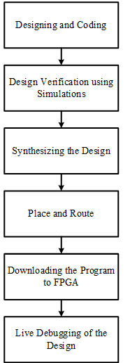
Figure 1: FPGA Design Flow
Designing and Coding
The first phase of any hardware design either Application Specific Integrated Circuits (ASICs) or the FPGAs is the designing and verification of the whole process on paper before starting the actual coding. For this purpose, the design can be broken down into many different sub-modules which are then used to construct the whole system. For this purpose, we will consider a simple example of 1-bit full adder. If you see the diagram of the adder below, it can be observed that the design can be broken down to different sub-modules.
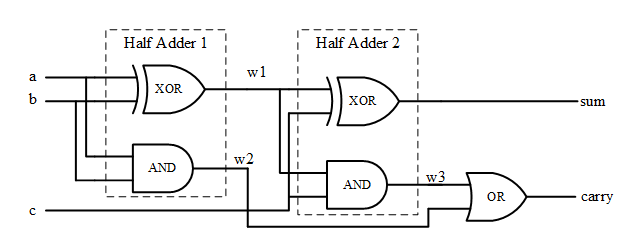
Figure 2: 1-bit Full Adder using Basic Building Blocks
The technique is known as bottom-up approach, where we start from basic building blocks and make a full model gradually.
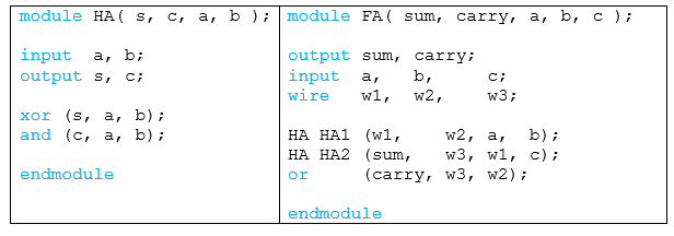
When the design process is completed, the code of the design model can be written in ModelSim or Xilinx VIVADO, which are some of the most common tools being used today. A sample code for this example is shown below.
The code on left side shows the half adder using two basic logic gates, while the code on right side shows the 1-bit full adder using half adder.
While creating the project, we can also select the model of FPGA which we are going to use for our design. In this way, it is possible to keep a track of the utilized resources of the selected FPGA.
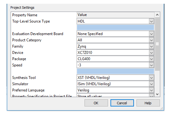
Figure 3: Selection of FPGA and other parameters for our design
Design Verification using Simulations
The second important step of the FPGA design process is the verification of the model which was designed in previous step. For this purpose, a testbench is written. The best practice to write a testbench is to add all the possible combinations of inputs and check corresponding outputs. These test values also include worst case test values as well. For the test case above, the testbench is shown in table below.
| module tb_FA;
// Inputs reg a, b, c;
// Outputs wire sum, carry;
// Instantiate the Unit Under Test (UUT) FA Unit_Under_Test( .sum(sum), .carry(carry), .a(a), .b(b), .c(c));
initial begin // Initialize Inputs a = 0; b = 0; c = 0;
// Wait 100 ns for global reset to finish #100;
// Adding Test Signals #10; a = 0; b = 0; c = 0; #10; a = 0; b = 0; c = 1; #10; a = 0; b = 1; c = 0; #10; a = 0; b = 1; c = 1; #10; a = 1; b = 0; c = 0; #10; a = 1; b = 0; c = 1; #10; a = 1; b = 1; c = 0; #10; a = 1; b = 1; c = 1;
end
endmodule
|
When the testbench is ready, the next step is to verify the results using simulations. For this purpose, the Xilinx IS simulator, ModelSim simulator can be used. A sample result can shown in figure below, where we can verify the output result for any corresponding input.
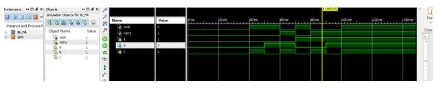
Figure 4: Simulation results for 1bit full adder using Xilinx ISE
In the results figure above, we can observe that the code shown above provides a correct result. For the part selected in simulations, we can also observe that we have 101 as input and carry is 1 while sum is 0, which is correct result.
Synthesizing the Design
The next step is to synthesize the design. In this step, a high-level design is converted to basic blocks which is implemented on the FPGAs. For the above example, the code is synthesized and the RTL schematic is shown in Figure 5.
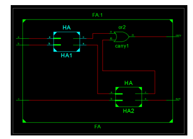
Figure 5: RTL Schematic of 1 bit full adder
While we can also view the technology schematic in Xilinx which represents the schematic which is going to be implemented on to the FPGA. The technology is shown in Figure 6.
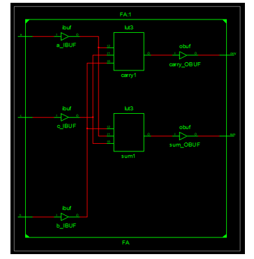
Figure 6: Technology schematic of 1-bit full adder
In the figure above, we can observe that the complete design is now translated to Look-up-Tables (LUTs) where one LUT deals with sum and the other with carry.
Design Implementation
This is considered as the most important step after the design phase. In this phase, three steps are performed: (i) Translate, (ii) Map, and (iii) Place and Route.
In the translation step, the top-level code is translated to gate level primitives which are then used to implement the design on FPGAs. If one doesn’t take care while coding, this can effect the translation step as it may generate the latches in the design and the performance will be effected. To overcome this, one rule to follow is to design your code such that it can handle all possible inputs.
The next step is to map the translated code to a specific library in FPGA. So, for this purpose MAP step is used.
The last step is to place and route the design onto FPGA. For the sample code, the place and route is shown in Figure 7.

Figure 7: Image on Left side shows complete FPGA while on right side the block of 1-bit adder is shown
The image on left side shows complete FPGA while a red dot, which is barely visible, within the yellow surrounding shows the 1-bit full adder. If we dig into the red block, we can see the actual translation of the code onto FPGAs. The translated circuit is shown in Figure 8 below.
Figure 8: Place and Routed 1-bit adder on FPGA
Using the Xilinx’s tool we can also investigate the design utilization report for the design. We can check which source are available and how many are used for this current design. Here we can see that this current design uses 2 LUTs which were also mentioned in technology schematic above.
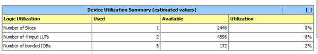
Figure 9: Device Utilization Report
Downloading the Program to FPGA
To download a code to the FPGA, it is important to first generate a bitstream which helps FPGA read the required instructions. The next step is to download the code to FPGA. For this purpose, Xilinx, or third party tools can be used which help to download the bitstream, which was generated using Xilinx onto FPGAs.
Live Debugging of the Design
There are different tools which provide options where an engineer can test the working of the design while it is on FPGA. This is called on-chip debugging. For this purpose, ChipScope Pro is a tool from Xilinx which is preferred. One can add triggering points and view internal signals of FPGA onto the computer screen. This helps debug the code even after the code is downloaded onto FPGAs.
FPGA Design Optimization
For an FPGA design, there are different performance factors which should be kept in mind including (i) latency, (ii) speed, (iii) area, and (iv) power. While optimization, there will always be a tradeoff between there parameters as if we optimize for speed, the power consumption and area utilization will be high. While we work for area, then the power and speed will be compromised.
Speed is important for real time applications and the applications where we are dealing with data processing. If we have to optimize the speed, then we have to work on pipelining. The pipelining can boot the speed of the design up to two times.
As far as the area reduction is concerned, we can reduce the side of area but for that we have to compromise the speed of the design. But considering the applications the speed of the design is considered as the most important factor for many applications. So, speed it normally, not compromised, but on the other had the area size of the design is increased. This results in increased manufacturing cost for FPGAs.
FPGA Tools
Here is a list of tools which are useful for FPGA design:
Coding and Simulations
- ModelSim (https://eda.sw.siemens.com/en-US/ic/modelsim/)
- Xilinx ISE (https://www.xilinx.com/products/design-tools/ise-design-suite.html)
Synthesis and Implement Design
- Xilinx ISE (https://www.xilinx.com/products/design-tools/ise-design-suite.html)
- Quartus II (https://fpgasoftware.intel.com/13.0sp1/)
Download Code to FPGA
- Xilinx ISE (https://www.xilinx.com/products/design-tools/ise-design-suite.html)
- Quartus II (https://fpgasoftware.intel.com/13.0sp1/)
- Digilent Adept (https://store.digilentinc.com/digilent-adept/)
On Chip Debugging
- ChipScope Pro (https://www.xilinx.com/products/design-tools/chipscopepro.html)
FPGAs and Prototyping Boards


