Understanding Full-Wave Rectifiers
21/05/2022, hardwarebee
The rectifiers can be classified into half-wave and full-wave rectifiers, and in this article, full-wave rectifier characteristics and applications are presented comprehensively. Then, a brief comparison between a half-wave rectifier and a full-wave rectifier is discussed.
A rectifier is a type of converter which converts AC parameters to DC ones. To achieve this aim, a circuit must be used to rectify the current or voltage. The simplest and most common type of semiconductor is a diode. Since there is no control over turn on and off conditions of the diode, the diode-based rectifiers are known as uncontrolled rectifiers. In fact, the diode turns on when the voltage across the diode goes higher than the threshold. And, the diode turns off when the voltage comes below the threshold value. Thus, the user cannot control the diode conditions. The threshold value depends on the diode material and manufacturer. However, the threshold value of silicon diode and germanium diode are around 0.7V and 0.3V, respectively. Other types of semiconductors are thyristor, metal–oxide–semiconductor field-effect transistor (MOSFET), insulated-gate bipolar transistor (IGBT), and so on. As the rectifier principles are discussed in this article, the diode-based rectifier will be explained.
A diode is an uncontrolled semiconductor element that allows the current to flow in only one direction and prevents the current in the reverse direction. The diode is presented schematically in Figure 1. Most semiconductors are made of silicon, but germanium is also used for more accurate applications. This semiconductor device has two terminals, including an anode (positive) and a cathode (negative). When the anode voltage is greater than the cathode voltage, the diode is in forward bias and acts as a close switch. However, the diode is in inverse condition once the anode voltage is less than cathode one (open switch). Thus, there is no external control on diode operations except voltage level in the diode terminals.
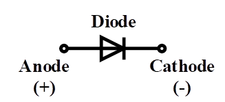
Figure 1: Diode terminals
Center-tapped Transformer Configuration
The half-wave rectifiers have high ripples and low average values, which are undesirable for some applications. Hence, the rectifier performance can be improved by developing the half-wave rectifier into the full-wave one. There are two configurations for a single-phase full-wave rectifier, including a center-tapped transformer and a bridge circuit. The main disadvantage of a half-wave rectifier is that the diode is off in a half cycle of input voltage, and the output voltage is zero in that half cycle, which decreases the rectifier performance considerably. Thus, if another diode is added to the circuit to turns on in the mentioned half-cycle, the rectifier parameters will be enhanced significantly. The first configuration that is presented in this article is a center-tapped transformer which is the modified version of a half-wave rectifier. As can be seen in Figure 2, there are two diodes in this configuration which means that the full-wave rectifier has higher costs. Moreover, the center-tapped transformer is more complex.
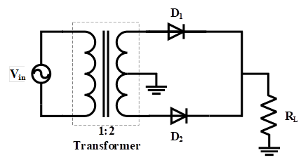
Figure 2: Using center-tapped transformer for a full-wave rectifier
The transformer turns ratio in this configuration is 2, which means that the voltage of each half winding is equal to the input voltage, as shown in Figure 3. In the positive half cycle, D1 is turned on because the voltage at the anode point is greater than the cathode point, and inversely, D2 is off as the voltage across the diode is negative. Thus, the current flows through D1 and then passes the load resistance.
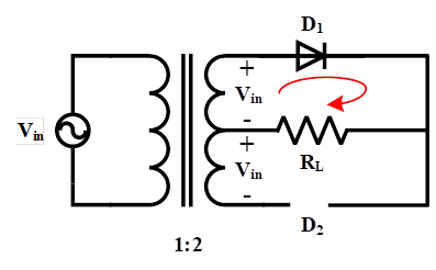
Figure 3: Center-tapped transformer configuration in the positive half cycle
In the negative half-cycle, D1 gets off, and D2 turns on, as shown in Figure 4. In this condition, the secondary voltage is applied to the load resistance because D2 is in the forward bias. It is worth noting that the diode is considered an ideal one in which its voltage drop is zero. In both cases, the current direction that flows through the resistance is the same, and the voltage is not zero in each cycle. Therefore, by applying a sinusoidal voltage to the transformer primary, the output voltage across the load resistance would be similar to the waveform presented in Figure 5.
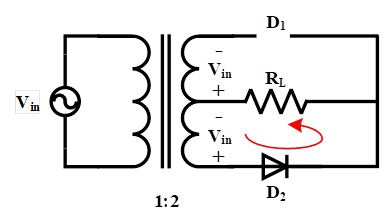
Figure 4: Center-tapped transformer configuration in the negative half cycle
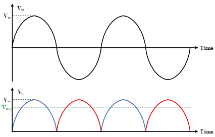
Figure 5: Input and output voltages in center-tapped transformer configuration
In full-wave rectifier, the output voltage can be written as:
(1)
where Vm is peak voltage, t is time, f is frequency, and T is the waveform period. In this situation, the average voltage can be calculated by:
(2)
It should be noted, in non-ideal condition, is replaced by Vm-0.7 because the diode voltage drop is around 0.7V. Moreover, the output frequency in full-wave rectifier is twice the half-
wave rectifier because the waveform period is T/2 where is the input waveform period. Therefore:
(3)
![]()
Another important parameter is diode peak inverse voltage (PIV) which expresses the tolerance level of the diode in reverse bias. In the positive half-cycle, D1 is conducting, and D2 is off. Thus, the voltage across D2 would be two-fold of input voltage. It means that the diode must tolerate when it is off. Choosing a diode with this voltage tolerance may increase the cost of the rectifier. Therefore, it can be written:
(4)
PIV = 2Vm
where is the peak value of input voltage. The situation is the same in the negative half-cycle, as D1 is off and D2 is conducting. The main drawbacks of the center-tapped transformer configuration are high PIV and complex transformer manufacturing. The other full-wave rectifier configuration is the bridge which consists of four diodes, one transformer connected to the voltage source, and load, as shown in Figure 6.
Full-Wave Bridge configuration
Despite the center-tapped transformer configuration, using a transformer is not a must in a bridge configuration, and the bridge can be connected to the voltage source directly. Therefore, the circuit size can be reduced by removing the transformer.
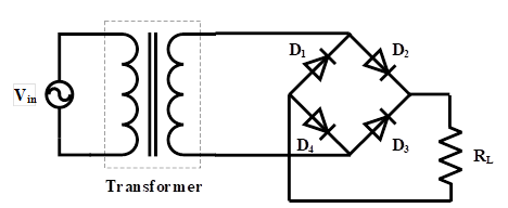
Figure 6: Full-wave bridge rectifier configuration with four diodes
In each half-cycle, two of four diodes are on, and others are off. During the positive half-cycle, D2 and D4 turn on, and D1 and D3 are off to feed the load resistance. The current flow in the positive half-cycle is illustrated in Figure 7.
Figure 7: Full-wave bridge rectifier in the positive half-cycle
In the negative half-cycle, D1 and D3 are on, and the current closes its path through these two diodes to feed the load. The current flow in the negative half-cycle is shown in Figure 8.
Figure 8: Full-wave bridge rectifier in the negative half-cycle
As this configuration is also a full-wave rectifier, the output voltage waveform would be as same as Figure 5, and the average value is 2Vm/Pi . However, in non-ideal diode condition, the average voltage would be 2(Vm+2*0.7)/ Pi because two diodes are available in each half-cycle which drops the voltage. The PIV for bridge configuration is equal to the input voltage, and it can be written as:
(5)
PIV = Vm
Full-wave Rectifier Parameters Calculation
This equation expresses that the voltage of diodes in bridge configuration is less than in center-tapped transformer configuration. Although a full-wave rectifier has better output, it has a ripple. This undesirable ripple can be reduced by adding a filter to the circuit. The filter is a capacitor in parallel with the load resistor. At first, the capacitor is completely discharged, and the input voltage is zero. In the positive half cycle, the voltage gradually reaches the peak input voltage. The empty capacitor acts as a short-circuit path and becomes charged in this condition. The voltage of the charged capacitor is equal to the peak input voltage. By passing the peak voltage, the input voltage becomes less than the capacitor voltage (Vm). Therefore, the diode turns off, and the capacitor is discharged to the resistive load. Due to discharging of the capacitor, the output voltage decreases to reach the next positive half cycle. This process is repeated periodically, as shown in Figure 9. The output voltage is the red line in this figure, and its ripple is considerably low.
Figure 9: Full-wave rectifier output voltage by considering capacitive filter
In full-wave rectifier, the peak-to-peak voltage ripple can be determined by:
(6)
where, f is input frequency, RL is load resistance, and C is the capacitor value. Furthermore, this ripple can be calculated based on the load current as:
(7)
![]()
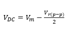
Also, the DC voltage after filtering can be obtained by:
(8)
What is the Ripple Factor of Full Wave Rectifier
Another parameter is the ripple factor which is the ratio of RMS voltage and DC voltage. Without the capacitive filter, the ripple factor of the full-wave rectifier is 0.482. In terms of efficiency, the efficiency of the full-wave rectifier is 81.2 percent which shows the ratio of DC output power and the AC input power.
Difference between Half Wave and Full Wave Rectifier
To sum up the article, Table 1 presents the discussed parameters for half-wave rectifiers and full-wave rectifiers.
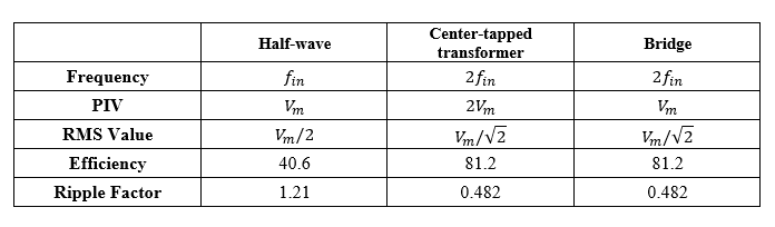
Evidently, the full-wave rectifier configurations have better performance than the half-wave rectifier, but more diodes are needed, and the rectifier size increase
The difference between output voltage in half-wave rectifiers and full-wave rectifiers is that the output voltage in the negative half-cycle is no longer zero, and the average voltage will be higher.