Understanding Sample and Hold Circuit
14/05/2022, hardwarebee
A sample and hold circuit is an analog device that takes the voltage of a continually changing analog signal and holds it at a consistent level for a set amount of time. The sample and hold circuits are commonly used to filter out anomalies in input signal, in Analog-to-Digital Converters (ADCs), which may impair the conversion. In a typical sample and hold circuit, a capacitor holds an electric charge, and at least one switching device, such as a field effect transistor switch, and generally one op-amp are added (operational amplifier). The sample and hold simplest circuit schematic is shown in Figure 1.
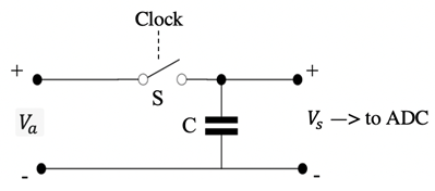
Figure 1: The simplest sample and hold circuit
Vs: Output signal
C: Capacitor
S: MOS transistor operating as a switch
Va: Input Signal
The clock pulse activates the switch (S). The input signal is sampled or retained at the most recently sampled values depending on the clock pulse. The input signal is sampled when the clock pulse is high, and the values are retained when the clock pulse is low. the circuit can operate in two modes, which depends on the logic level of the sample and hold clock signal. The input pulse for clock switching and the output of the circuit are shown in the figure below.
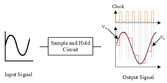
Figure 2: The switch clock pulse and circuit output
Why are Sample and Hold Circuits Necessary?
The output digital value is likely to be erroneous if the ADC’s input analog voltage swings by more than ± 1/2 LSB. For the ADC to work efficiently and deliver the correct results, the analog voltage at the input source should be kept constant during the conversion. In response to a sampling command, input analog signal is sampled by the sample and hold circuit and stores the output value until the next sampling command is received.
Types of Sample and Hold Circuits
Circuits for sampling and storing data exist in a range of designs and sizes. We are going to discuss some kinds of Sample and Hold circuits. It’s worth noting that each of the following circuits uses a JFET as a switch. In the circuits, the JFET is turned on during the sample time, and during this time the charge in holding capacitor reaches its maximum value which cannot exceed the input signal. When the sampling period is completed, the JFET turns off and the holding capacitor is disconnected from the input signal. By disconnecting the capacitor, it is ensured that the output remains the same as of the input voltage, and it doesn’t vary with the variation in input signal. It may be the case where the voltage across holding capacitor has a low dropout and to compensate those two buffers are used, one at the output and the other at the input.
The first type of sample and hold circuit is shown in diagram below which is known as open-loop type Circuit.
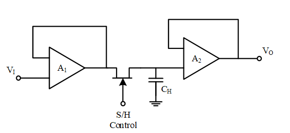
Figure 3: sample and hold circuit which known as open-loop type
Since this is an open-loop circuit, so it is considered as quicker sample and hold circuit than the other closed loop circuits. Because there is no feedback (closed-loop configuration) in this circuit, it is quicker than closed-loop circuits. Closed-loop designs, on the other hand, produce higher accuracy as a result of feedback. For sample and hold circuits, the acquisition time is a critical factor, and it must be kept as short as possible. The acquisition time majorly depends on three factors; (i) OpAmp slew rate, (ii) The maximum output current, which is achieved, and (iii) RC time constant, where C represents the holding capacitor and R represents the ON resistance.
The following feedback loop circuit is an improved variant of the previous one. Because the JFET’s ON Resistance is included in the feedback loop, the other two parameters determine the acquisition time.
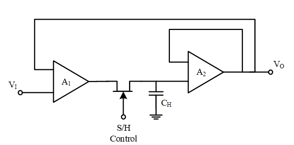
Figure 4: Closed-loop sample and hold circuit
By delivering voltage gain, the following circuit outperforms. To compute the circuit’s voltage gain, feedback resistor (Rf) and the input resistor (R1) can be used (the formula for voltage gain is given below).
A = 1 + (Rf / R1)
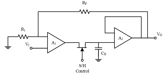
Figure 5: Closed-loop sample and hold voltage gain circuit
The last circuit provides a few advantages over the prior one. The most important change is the location of the holding capacitor, which results in equal voltage at non-inverting terminal of , and the voltage which is across the capacitor divided by the gain of amplifier. As a result, the holding capacitor charges faster, which leads to a faster acquisition time.
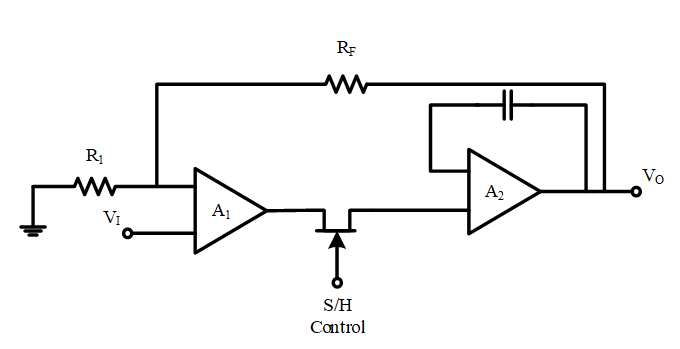
Figure 6: Closed-loop sample and hold Voltage gain circuit with non-inverting terminal
Sample and Hold Circuit Operation
A typical sample and hold operation circuit is shown below, with practical components.
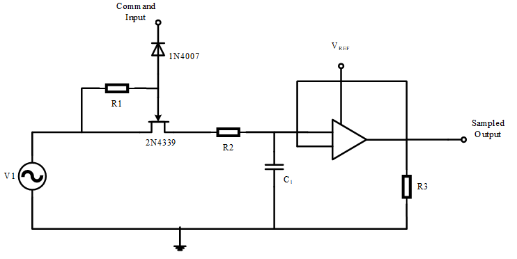
As indicated in the circuit design above, a capacitor, an op-amp, and an N-channel JFET is used. The 2N4339 transistor’s gate terminal is connected to a command input (a PWM input). To control the operation of the JFET, a diode 1N4007 is connected between the JFET and the command input.
The JFET used in this circuit is a low-noise N-channel JFET with a high gain. The conduction of JFET depends on the gate to source voltage, it only conducts when this voltage is between -0.3V and -50V (being 50 the maximum value for this JFET). For this circuit, the pulse value is set to 15V, and the beginning of the command input value is set to -15V. The diode is forward biased when the command input voltage is negative, pushing the transistor to switch on, and vice versa.
The circuit requires a voltage follower circuit, which is an Op-amp (741) in this circuit, because this Op-amp has low output impedance and a high input impedance. The voltage follower is employed when the input signal has a low current because it can give enough current to the following step.
The transistor shuts and the capacitor begins to charge to its maximum value when the command input is HIGH. This operation will store the sample of the input signal during the on state of the transistor. The transistor operates as an open switch, when the command input is LOW, which causes the capacitor to have a high impedance, which prevents discharge and allows the charge to be stored for a long time, and this is known as Holding Period. Every S/H circuit takes some time to sample the input signal, and this time is known as Sampling Period.
Performance Parameters
The quality of a sample and hold Circuit is measured using different factors which include, non-linearity, gain error, input offset voltage, and other amplifier-specific metrics. The sample and hold Circuits, on the other hand, have a few distinguishing qualities. All these characteristics can be used to assess the device’s performance during operations in hold mode and in the transition from sampling to hold mode. The diagram below can assist us in better understanding these qualities.
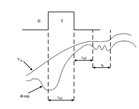
Acquisition Time (tac):
During sampling, the acquisition time is the time it takes for the charge in the holding capacitor to reach a level close to the input voltage. It is influenced by three factors:
- The RC Time Constant is a constant that is used to calculate the length of time
- The Op-Slew-Rate Amp’s is the rate at which the transistors in the transistors in the transistors in the transistors
- The Op-maximum Amp’s output current
Aperture Time:
It is a delay between start of the hold command and VO monitoring the Vi. Propagation delays across the driver and switch circuits are the most common source of this delay. The hold command must be started an aperture time ahead of time for optimal timing.
Aperture Uncertainty:
Aperture times is not consistent, and it varies from sample to another. This type of uncertainty is known as Aperture Uncertainty. This will have a significant impact on the hold command’s development.
Hold Mode Settling Time:
After the hold command is applied, the settling time for the output (VO) within a specific error band percentage (0.01%, 0.1% or 1%) is known as the hold mode settling time.
Hold Step:
The parasitic capacitances may cause an unexpected charge transfer between the holding capacitor and the switch, while switching from sample mode to hold mode. This has an impact on both the capacitor voltage and the output voltage. The Hold Step is the difference between the output voltage and the desired value.
Feedthrough:
In hold mode, the parasitic capacitances of the switch may produce AC coupling between VI and VO. Feedthrough phenomenon occurs, which causes the variation in output voltage with change in the input voltage.
Droop:
Voltage droop is developed when the leakage current drops the voltage across the holding capacitor.
Advantages:
- A traditional SH Circuit’s main advantage is that it can help in getting the ADC values while maintaining the sampled analog input voltage.
- If the analog samples from all channels are sampled at the same time, an sample and hold circuit can improve synchronization between distinct channels in multichannel ADCs.
- In multiplexed circuits, an SH circuit can be utilized to reduce crosstalk.
Applications of Sample and Hold Circuit
S/H circuits have a variety of uses. The following are some of the applications for such circuits:
- Analog to Digital Converters (ADC)
- Digital Interfaces
- Amplifiers for Operational Use
- Demultiplexers for analog signals
- Systems for distributing data
- Multiplexer outputs are stored.
- Pulse Modulation Systems (PMS) are a type of pulse modulation system
Conclusion
A sample and hold circuit in Analog to Digital Converters is a simple sample and hold circuit that employs a MOSFET and a Capacitor, as well as other types of Sample and Hold circuits, some important criteria that affect the performance of an sample and hold circuit, and sample and hold circuit applications.