The Ultimate Guide to FPGA Clock
30/01/2019, hardwarebee
Field Programmable Gate Arrays or FPGAs in short, have become one of the most popular choices among digital engineers, having already taking a big share of the market among microprocessors and ASICs. Not only do FPGAs offer an affordable and relatively less expensive alternative to these other traditionally used embedded systems, but they also boast added flexibility and efficiency, making them the prime option when it comes to small or medium size volume products.
FPGAs employ the use of several blocks or flip flops that work in parallel in different interconnecting paths that can be operated in different frequencies. Clocks are what make it possible for the various flip flops inside a single FPGA to transition to a new state at the clock speed, allowing FPGA to make high speed calculation or bit manipulation in high speed.
Clock in FPGA
A clock is a signal inside any digital circuit the determines how fast a flip flop (or a group of flip flops) runs. The clock signal is connected to all flip flops and RAM blocks and activates them according to the clock frequency. The faster the clock, the faster the design will run and therefore a higher clock speed FPGA will perform any desired function quicker than a slow clock speed FPGA. A typical FPGA consists of several clock signals and thus allows different areas across the FPGA to operate in different speed.
FPGA Clock Domains
FPGA systems contain internal phase locked loops of PLLs that help generate various frequencies of signal waves. A clock in an FPGA system is responsible for driving the FPGA design and determines how fast it can run and process data, with numbers reaching a maximum of upwards of 1GHz. it produces a fifty percent duty cycle of square waves that are half on off time and half on time. A faster clock translates into a faster data processing, but a fast clock is not what is always needed.

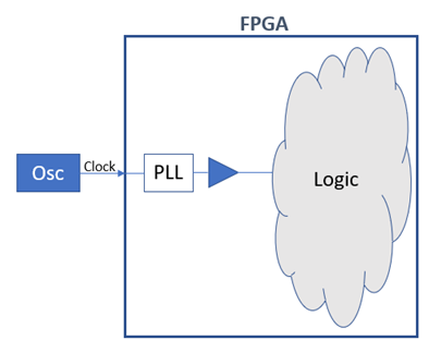
Figure 1: Illustration of a typical clock circuit in FPGA with one clock domain
A single FPGA system will employ the use of at least one clock that will generate a wave at a certain frequency which will then be distributed across the FPGA to produce a synchronized response from all the flip flops involved in the design.
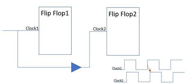
An external oscillator placed on the circuit board is what generates the square wave or clock signal with a certain frequency and enters the FPGA system through a single physical connecting pin. The clock signals are distributed along interconnected lined or wires called global routing or global lines so that the signal is distributed and received at the same time by each flip flop. If the signal reaches the different flip flops at different times, the time difference between the reception of the clock pulse is called skew and can interfere with the performance of the system. Therefore, employing the use of a clock with dedicated routing helps avoid skew or minimize it to the maximum possible degree.

Figure 2: Skew in clock signal distribution caused by delay in clock wiring
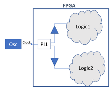
Each clock domain will have its own dedicated routing and clock pin, with the entire system termed as a single block with extremities that extending all the way to all of the flip flops, almost like a tree branching out.

Figure 3: FPGA with 2 clock domains running 2 separate clock speeds
You may think about using multiple clocks if you are using an external device such as an SDRAM, Sensors, Camera, or any other special external components that need another signal at a different frequency in order to run directly in association with your FPGA. but you have to consider the fact that managing multiple clock domains in a single FPGA is really complicated and should generally be avoided when possible, which is the case in this situation.
PLL in FPGA
You do not have to use multiple FPGAs every time because you can actually use a single clock domain to generate multiple frequencies of waves and run different components. The part of your FPGA that you
will have to refer to do in order to do this is the PLL or the Phase Locked Loop. The Phase Locked Loop takes the reference clock and spins it up to generate a very high frequency in Giga Hertz in accordance with the clock you require for your equipment. This means that you can manipulate the code to change how often your clock enabler gets pulsed and so determine the frequency of the resultant signal waves. Instead of getting a dedicated clock for everything, you can simply take a clock that has, for example, a wave frequency of 50 MHz, and then have it pulse every so often per number of cycles to get a customized clock with variable frequencies.
Crossing Clock Domain in FPGA
If you have to transfer data across multiple clock domains, then you must look into crossing them using the likes of synchronizers or FIFOs. Two completely different clocks cannot use each other’s signals if they are not related at all as it would induce an element of metastability. Splitting and crossing the clock domains in your FPGA can end up producing unwanted glitches bugs that can end up being extremely difficult to understand and remove. Not only that but using logic in order to create multiple clocks can introduce skew into your designs as you will be using routing fabrics instead of dedicated clock routing lines, with the former having a greater number of interconnects which cause the signals to become lethargic and variable. At the end of it all, this system can end up being extremely inefficient as well as highly power consuming if you are not aware of how to properly cross the clocks or manage them.
Therefore, if you are just a beginner, it is better to simply stick to a single clock domain and modify it to suit your flip flops as handling and organizing multiple clock domains is an extremely complicated task that must be monitored carefully and managed meticulously so that you do not end up with problems you cannot handle or understand.


