
Understanding FPGA Programming and Design Flow
28/10/2019, hardwarebee
Find electronic design, board design and module design companies:
Find FPGA design companies:
Find embedded software companies:
This article will brief you on how to perform a full hardware implementation on FPGA. However, before we get to the FPGA design flow, let’s discuss first why you would choose to use an FPGA.
There are 2 ways in which you can develop chips: ASIC (Application-Specific Integrated Circuits) and FPGA (Field-Programmable Gate Arrays). Although ASIC can be quite efficient in terms of design area, power and speed, it can be very exhaustive in terms of time consumption and resources. It could take a long time to manufacture a custom chip from scratch, as well as a require high investment. Therefore, as long as the desired product is not needed in bulk amounts, FPGAs would be mostly the more adequate choice.
Now, getting back to the actual FPGA design flow. The process goes as demonstrated below in figure 1.
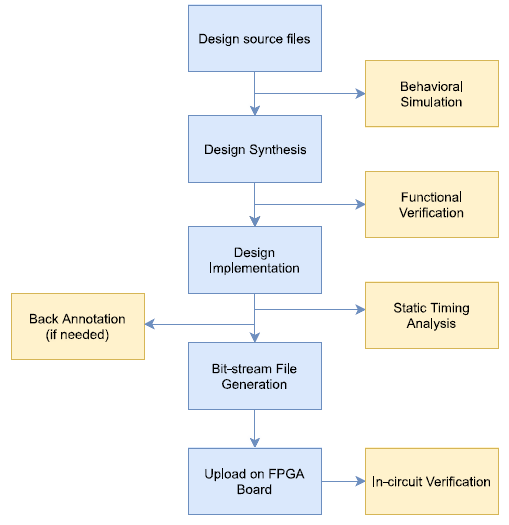
Figure 1: FPGA design flow
FPGA Design Specifications
First, determine the FPGA design functionality and power/area/speed specifications. The design architecture is then created based on these premises. The architecture would be normally partitioned into sub-modules that interact with each other to form the system level module. This hierarchical organization makes it easier to do team work, trace behind errors and re-use modules for other designs.
As an example, we will chose to implement a full adder design on FPGA. Figure 3 represents a hierarchical design of the full adder, which is composed mainly of 2 cascaded half adders. The design structure of the half adder is shown in Figure 2 and 3.
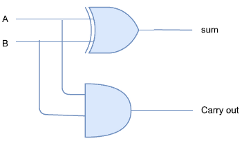
Figure 2: Half adder schematic design
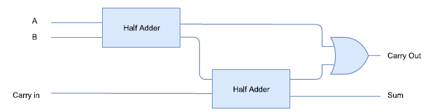
Figure 3: Full adder schematic design
In this stage, also, the FPGA development board on which the design will be uploaded should be chosen. The design requirements, including the number of logic units, flip-flops, memory capacity and so on, in addition to the available price budget determine which FPGA board would be suitable for the implementation. In this article, I will be synthesizing and implementing this design on UltraScale Kintex+ platform using Vivado Xilinx tool.
FPGA Design Entry
There are different formats in which the design source files can be represented. Files could be uploaded to the FPGA CAD tool in schematic format, which is easier to read and mainly more efficient for smaller designs. Design files can also be represented in hardware language (HDL), which is more suited for complex systems. Here, we choose to represent our full adder in HDL, so we input the source codes along with the constraint files to the CAD tool at this stage. The Verilog code in figure 5 describes the structure of a full adder. The circuit adds 3 bits, carry in and inputs, and outputs sum and carry out. The full adder is designed as a top module that makes 2 instantiations of the half adder sub-module, shown in figure 4.
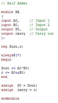
Figure 4: Half adder Verilog code
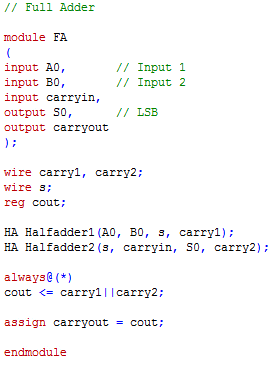
Figure 5: Full adder Verilog code
Design Constraints are also written in an XDC file, as illustrated in fig 6. The most important constraint is the clock. Each FPGA platform has a different pin assignment for the clock. The reason for this is clock needs a designated high speed pin to be able to generate correctly. Also, In UltraScale platforms, the clock can be chosen to be input differentially. Here, I chose a clock speed of 250 MHz and a differential IO standard to match my differential clock. The package pins should also be assigned for proper placement.
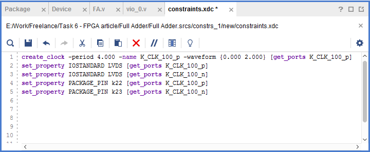
Figure 6: Design Constraints
FPGA Behavioral Simulation
Next, the behavior of the Verilog code is verified by running the behavioral simulation, which would display the waveform of the inputs and outputs. Different combinations for the inputs can be tested to make sure that the code is working properly. This stage is only to ensure that the code is free of bugs. Using the behavioral simulation tool in Vivado, the design behavior can be verified as shown in figure 6. All possible inputs of a 3-bit full adder are shown, for example; the result for 1 + 1 is represented in binary as 1 for the carryout and 0 for S0. Test benches would be recommended for large design to test more, however, this waveform can be accessed by manually assigning values to input ports in the window shown on the left in figure 7.
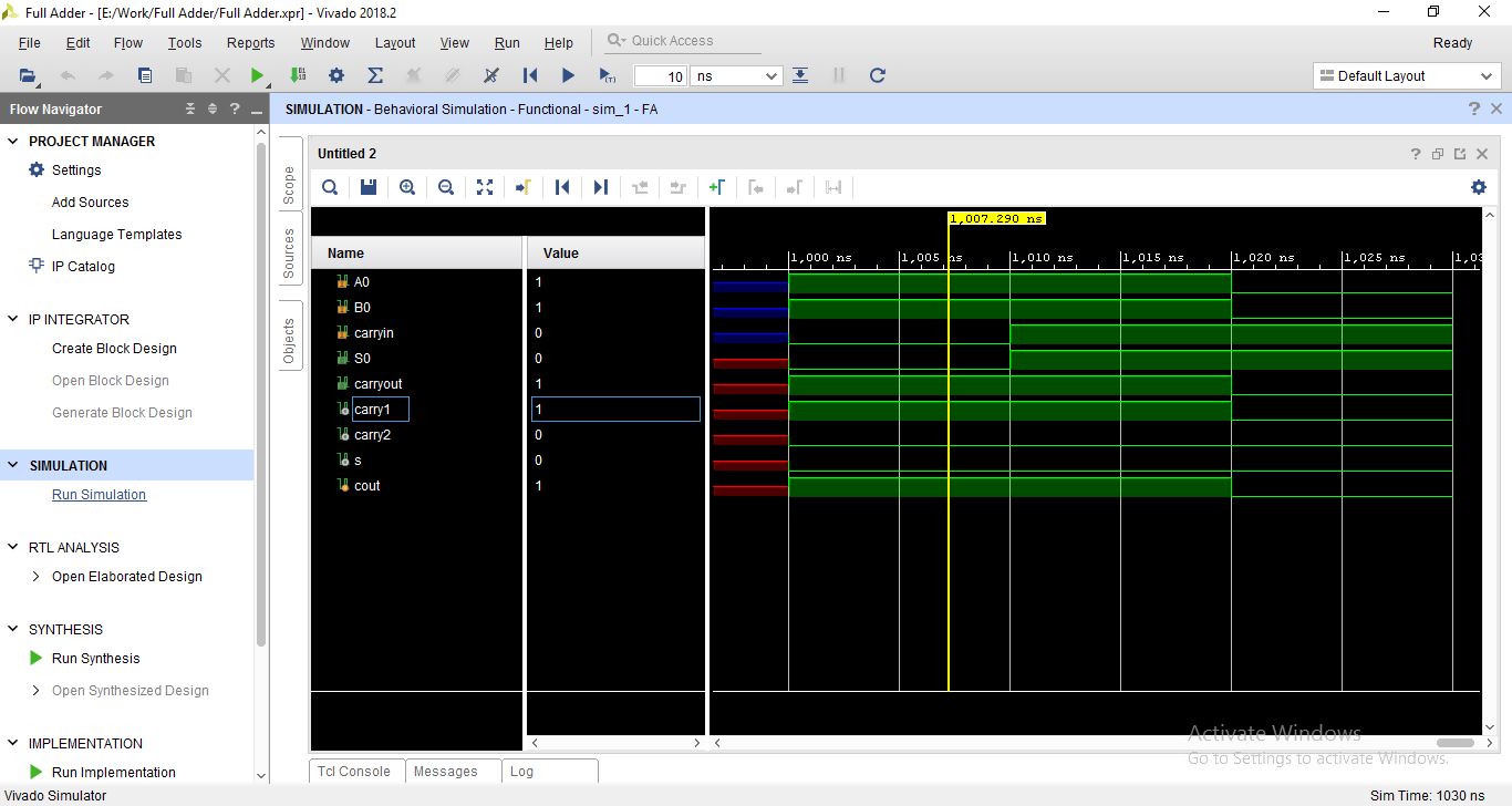
Figure 7: Test Bench of the full adder Verilog code
FPGA Design Synthesis
Verilog source codes and design constraints, including timing and physical constraints, are then fed to the synthesis tool. Constraints are added to ensure that functionality and performance of the design are as required by the designer. The tool transforms the RTL code into a gate-level description that undergoes logic optimization and reduction. The logic gates are then mapped to existing technology libraries, so that we eventually can have an optimized gate-level netlist that the next tool can understand. At this stage, reports containing information about cell usage, area and timing are also created and are output to the user, so that they can be checked for improvements or violations to any of the design constraints. The output of this stage is a netlist of the synthesized modules as shown in fig 8, this is used to check if all intended blocks are actually synthesizable. Figure 8 demonstrates that all the modules are synthesized.
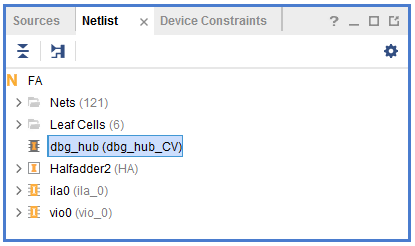
Figure 8: Design Synthesis Netlist
FPGA Design Implementation
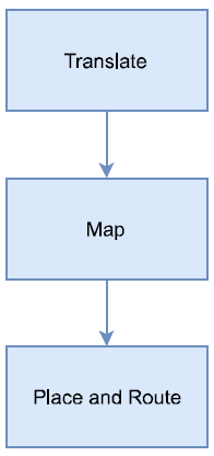
Figure 9: The 3-stage implementation process
The implementation phase is a 3-step process, as elaborated in fig 9. First comes the translate stage, which combines all previously produced netlists and constraint files into one large file. It also does port assignments to actual FPGA pins, switches and buttons, while respecting design constraints. The next stage is the map phase that divides the netlist into sub-blocks and maps them to actual FPGA blocks. Finally, the last stage is place and route. It places the design sub-blocks in their designated FPGA blocks, then routes between the blocks. The placement and routing should be done while considering time constraints, for example; placement near the I/O pins can help save time.
Static Timing Analysis
Static Timing Analysis (STA) is carried out after the design implementation to check that the design follows the timing constraints. It checks all the possible signal propagation paths for delays. It then reports the longest possible delay, named as the critical path, to make sure it does not violate the desired timing performance. STA also checks for hold-time and setup-time violations and reports any breach. Fig 10, shows the timing summary of the implemented design with all constraints met and the worst negative slack, which represents the circuit’s longest delay path. The slack is positive and it meets frequency of operation of 250 MHz.
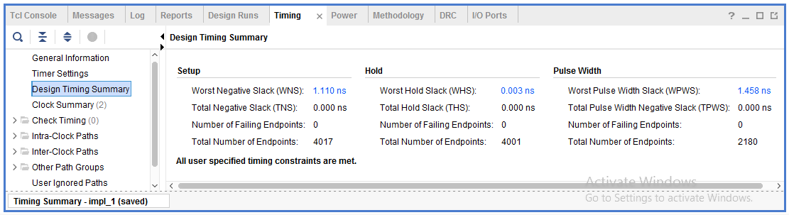
Figure 10: Timing analysis
Back-annotation
This step checks the reports produced after the implementation phase for violations or improvements to be made. In case of Timing or physical constraint violations, either the constraints or the design itself would need to be edited. Afterwards, design is re-synthesized and re-implemented. This process goes on repeat until all design rules are eventually met.
Bitstream File Generation
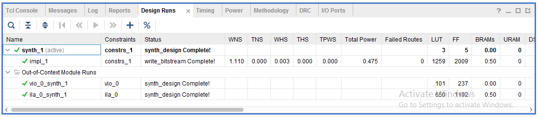
Figure 11: Full Design Implementation Complete
The implemented design must then be converted into a Bitstream, using a bit-generation tool, so that the FPGA platform can understand the design. The Bitstream file is then stored on the FPGA memory card, so it can be uploaded by the board. As demonstrated in fig 11, the full design process in successfully completed and the Bitstream file is generated successfully. The board should be connected to your device using a USB. The Bitstream file could then be used to program the board directly through the hardware manager.
In-circuit Verification
After the Bitstream file is uploaded on the FPGA, in-circuit verification is carried out to ensure that correct circuit implementation has taken place. This is done using the hardware debugging IPs integrated in the FPGA board. As shown in fig 12, I used a Virtual Input/output (VIO) to drive my inputs: A0, B0 and carrying into the design. Also as demonstrated in fig 13, I used an Integrated Logic Analyzer (ILA) to monitor my outputs: S0 and carryout. VIO and ILA module can be instantiated from the IP catalog. The setup and number of ports required can be controlled from the IP settings.
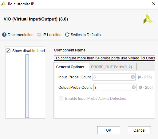
Figure 12: VIO IP Settings
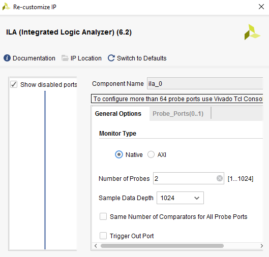
Figure 13: ILA IP Settings


