Understanding Edge AI Architecture
28/10/2021, hardwarebee
According to new research by Markets and Markets, the edge AI hardware market is anticipated to ship 1560 million units by 2024, growing at a CAGR of 20.64 percent during the forecast period. However, the effectiveness of modern AI approaches is based on computing. A superior AI system’s training may take a month and cost $100 million.
CPU chips not only have the most transistors (basic computer components that can be switched between (1) and (0) states) but they can also be customized to efficiently execute certain AI system computations. Processor chips provide this massive commutative power.
The usage of standard AI chips or general-purpose CPUs for economically effective, wide-ranging AI deployments may cost you tens to thousands of times more for such cutting-edge ‘AI’ processors.
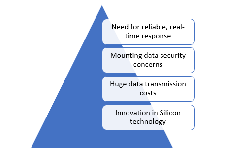
Figure – 1: Factors driving accelerated adaption of Edge AI solutions
This article explains the common AI edge chip architecture and building elements and their purpose/duty. Also, the article discusses AI edge chip operation, and what are the benefits and drawbacks in comparison to the current situation? How will it be possibly utilized in the future?
Architecture and basic building blocks of AI edge chips
AI chips, such as general-purpose CPUs, enhance speed and efficiency by employing a growing number of smaller and smaller transistors, which operate quicker and spend less energy than large transistors. However, unlike CPUs, AI chips include additional AI-optimized design features. AI systems require identical, predictable, and independent calculations, which are significantly accelerated.
Because each job places distinct demands on processors, various AI chips may be used for training rather than inference. To begin, different data formats and models are more suited for training vs deduction, as training requires extra computational processes in addition to those shared with inference. Second, although parallel data almost always improves training, it does not necessarily benefit deduction. For example, a single data item can be inferred at the same time. However, for some applications, several data pieces can be inferred in parallel, particularly when the application requires a quick deduction of numerous independent data pieces.
Third, the relative importance of efficacy and speed may vary depending on the application for training and deduction. The cost-effectiveness and speed of iteration are critical for the training, efficiency, and speed of AI researchers. Rapid decrease in inference may be crucial, as some AI applications require real-time data classification on critical (e.g., autonomous automobiles) and impatient (e.g., mobile photo classifying) systems. On the other hand, the usable deduction speed may be limited. For example, the mobile app does not have to be faster and more trustworthy, which takes less time than the user reaction time.
Because inference chips have to optimize for fewer calculations, scientific breakthroughs are less important than training chips. In addition, while research costs are lower than GPUs and FPGAs, design engineers are assessing far fewer variables because ASICs are specially developed for certain algorithms. A computer technician can transform the circuit into an optimum circuit to construct a circuit for just one calculation. However, the engineer must predict which circuit will be most suitable for several activities, many of which at the outset are not known. When building a circuit for a variety of computations.
The entire capabilities of an AI chip have been used to promote it. GPUs and FPGAs have been widely sold for many years. Meanwhile, ASICs are more difficult to sell because to high design costs and restricted volume due to specialization. Despite delayed general-purpose chip advancement, a customized chip is significantly more inexpensive since it has a longer useful lifetime before subsequent generation CPUs attain the same speed or efficiency. When an AI chip is 10-100 times quicker at a period when CPU improvements are slow, then merely 15,000-83,000 sales volumes are needed to make the AI chip more affordable. The anticipated increase in the market size of AI chips may offer the necessary economies of scale to make AI ASICs even more efficient.
AI chips range in strength from more powerful to less powerful in different classifications. In high-end data centers, upside-down server-grade AI chips are typically used, and they are larger than other AI chips after packaging. Customers in the intermediate segment often use PC-grade AI chips. Mobile AI processors are often used to infer and are included in a CPU-based system at the low end. A mobile system must be scaled down to fit mobile devices. For each of these classes, the AI chip market share rose at the expense of the non-AI chip market share.
AI is restricted, but increasing, in importance to supercomputers. Server grade processors are typically deployed in data centers and can be run in a configuration known as “grid computing” sequentially or concurrently. A supercomputer uses processors, physically co-locates and interconnects them and uses costly cooling to prevent overheating. This technique enhances speed and greatly reduces effectiveness and is, in many cases, an acceptable tradeoff that needs rapid examination.
Few modern AI applications need extra higher-speed expenditure, yet training or inference for large AI algorithms is frequently so slow that supercomputers are only employed as a last option. As a result, whereas supercomputing chips are often employed by CPUs, the number of AI chips is expanding. GPUs accounted for the majority of worldwide supercomputer additions in 2018.
AI chips are often defined as graphics processing units (GPUs), field-programmable gate arrays (FPGAs), and a special type of application-specific integrated circuits (ASICs) designed for AI computations. A GPU, an FPGA, or an AI-specific ASIC that serves as the core of a system-on-a-chip is also included in this definition (SoC). Algorithms may be implemented in a variety of devices, including overall systems such as Central Processing Units (CPUs), but because of their importance, we will concentrate on GPUs, FPGAs, and AI-specific ASICs.
Algorithms for AI may work for other types of chips, such as General-Purpose chips (CCU), but we in this paper are focused on architecture based on GPUs, FPGAs and AI-specific ASICs as they are necessary to perform state-of-the-art AI algorithms efficiently and quickly.
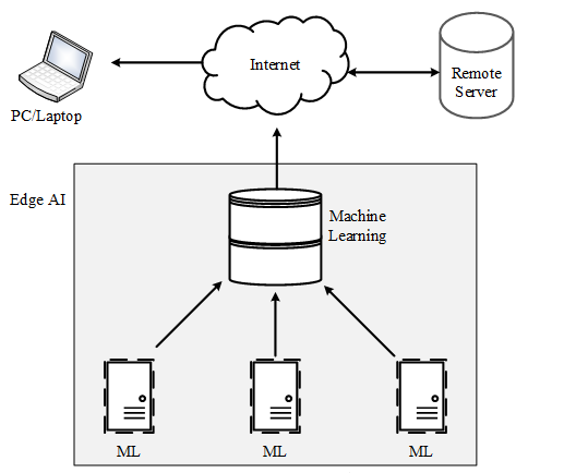
Figure –2: Basic building blocks of Edge AI
Graphics processing units (GPUs)
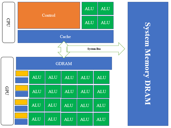
Initially, GPUs were meant for parallel computing application processing. GPUs were utilized in 2012, for the first time, for AI systems, and were acquired by 2017. In certain situations, GPUs are also inferred. Although the GPUs offer higher parallelism than the CPUs, they are still intended for processing for graphical purposes.
A GPU is made up of multiple processor clusters (PC), which include many streaming multiprocessors (SM). With its matching cores, each SM adopts a layer-1 cache. Before pulling GDDR-5 data from global memory, one SM typically uses a dedicated cache for layer one and a shared cache for layer two. Its architecture can tolerate memory delays.
A GPU is made up of many blocks, including numerous streaming multiprocessors (SM). Each SM uses a laying-1 cache with its corresponding centers. Normally, one SM will extract GDDR-5 data from global memory utilizing a specialized cache for the one layer and the shared layer 2 caches. Its memory delay resistant architecture.
Field-programmable gate arrays (FPGAs)
Specialized FPGAs and ASICs have recently become increasingly prominent for the deduction because of enhanced efficiency in comparison to GPUs. FPGAs feature logical blocks (i.e. modules that comprise a set of gates, each of which may be changed to fit certain algorithms by a programmer after manufacturing).
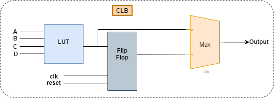
The basic FPGA architecture is made up of three different sorts of modules. I/O blocks or Pads, Switch Matrix/Interconnection Wires, and Configurable logic blocks are the three types (CLB). The basic FPGA design consists of two-dimensional arrays of logic blocks with an interface that allows the user to configure the connectivity between the logic blocks. The following are the functions of an FPGA architectural module:
- Digital logic, inputs, outputs, and CLB are all included (Configurable Logic Block). It takes advantage of the user’s logic.
- Interconnections provide guidance for the implementation of user logic between logic blocks.
- Depending on the logic, the switch matrix permits interconnects to switch.
- I/O Pads for external connectivity with various applications
Figure- 3: Logical internal Design of FPGA
Application-specific integrated circuits (ASICs)
An ASIC is a device with design engineers as a function to fulfill the demands of a certain application. ASIC stands for an integrated circuit customized to the application. ASICs permit the implementation of DSP algorithms in a specific, defined function logic to reduce the final energy usage and the hardware footprint.
An official classification of ASICs is a little hazy around the edges. However, four major categories are usually recognized: gate Array (GA) devices (including sea-of-gates), structured ASICs, standard cell parts, and full-size Custom components. There are also a few tiny rapscallions. In the early days of digital integrated circuits, there were just two devices.
An official ASIC categorization at the edges is kind of fuzzy. Four basic categories of devices structured ASICs, standard cell components, and customized full-sized pieces are commonly recognized: Gate Arrangement (GA) devices. A few tiny rapscallions are also present. In the early days of digital integrated circuits there were basically just two devices.
AI Edge Chip Architecture Comparison
There is no standard method for comparing CPUs and AI processors in this industry since the benchmark is based on chip performance and efficiency. However, at every node, AI chips frequently improve efficiency and performance by 10-1000 times over CPUs, with GPUs and FPGAs at the bottom and ASICs at the top. A thousand times as effective AI chip as a CPU for a given node improves the CPU over a 26-year period. Table 2 shows the estimations for DNN training and inference at the specific node for efficiency and performance improvements for GPU, FPGA, and ASIC linked to CPUs (normalized at 1x). FPGA training efficiency and speed statistics are unavailable due to the inaccessibility of FPGAs.

Table 1: Comparison of cutting-edge AI processors with the latest in CPUs
Related content: Edge AI overview

