FPGA Programming Tutorial
30/03/2020, hardwarebee
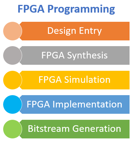
This FPGA programming tutorial shows the must-follow FPGA programming steps to ensure that there are no pitfalls in the programming and execution of the FPGA. The tutorial is starting with a introduction to the FPGA technology and then describes the programming process of an FPGA. This FPGA programming tutorial will cover all you need to know about the FPGA programming process and flow.
FPGA stands for Field Programmable Gate Array and is one of the most frequently and widely used and implemented kinds of semiconductor chips across a wide array of applications and industries. In recent decades, the applications of FPGAs have only grown, and it is has become as one of the most effective and efficient ways of generating low cost yet high-performance prototypes. But as simple and convenient as it sounds, the benefits of FPGA are not fully utilized without deep understanding of the FPGA programming process.
FPGA Design Language
When it comes to FPGA programming, one of the most important parts is the design language. This is the medium using which you will communicate with your technology and tell it what you want it to do. Using this language, you will basically be defining the operations of the hardware of that particular semiconductor chip and the device it powers. In the modern day, there are a huge number of computer design languages that can be used for this purpose.
Normally, you will use any hardware description language, or HDL, in the process of FPGA programming. You can use low level languages for circuits having relatively lower capacity. Higher end languages such as VHDL and Verilog which are used for higher complexity circuits and devices. Other factors that play a part in deciding which language to use include previous experience, personal preference and expertise, availability of models, synthesis capabilities, financial restraints, and hardware design.
FPGA Design Entry
The very first step in the programming of FPGA is the design entry. You have to enter or create the design that you have created for your FPGA into a dedicated EDA tool. There are multiple modes which you can use to enter a particular design into the tool. Circuit schematics mean you are presenting a graphical perspective of the design using logic gates and interconnects. Boolean expressions are written in text using logic designs in combination. HDL design, as explained before, uses a hardware description language to express the logic circuit in a text form. Lastly, you can also use state transition diagrams to present a graphical view of the state machines which can be identified as design states and the transitions between them.
FPGA Synthesis
The next process to come is the synthesis of the actual chip. Since the design has been fed into the tool and processed. The source files that are written in a particular language or format must now be processed and converted into a netlist by the program.
What is a netlist? A netlist is essentially a list of the elements that constitute the design of the chip as well as the connections between each of them. There is no hierarchy in the netlist as it is just an amalgamation of all the flip flops and gates used in the design.
There is optimization at the RTL, logic, and gate levels, and ultimately, a technology dependent netlist is produced from the initial HDL description. This netlist is then converted into a programmable logic device (PLD) or Field Programmable Gate Array (FPGA).
There are multiple tools available for the purpose of FPGA synthesis, inducing FPGA Express and the Xilinx Synthesis Tool.
FPGA Simulation
One the FPGA hardware design has been created; designers can stimulate the design to ensure that it works as it is intended to. In this simulation, the appropriate input is fed into the virtual FPGA chip and the outputs are recorded and compared to the expectations. This simulation can be done either using an interactive waveform editor or a testbench.
Making it a practice to run a simulation after each module to ensure that you catch bugs early and that your FPGA is fully functional and effective in accomplishing its purpose by the end of the process.
FPGA Implantation
Once the netlist has been created and tested, the design then needs to be translated and mapped out on a physical FPGA to create the appropriate pattern. This part of the process can be performed using many available tools such as Xilinx ISE or Altera Quartus II by Intel. This process can be divided into three stages.
- Translation: The translator collects all the netlists, creates a master netlist, and then verifies the constraints of the signals.
- Mapping: The mapper compares the resources specified in the great netlist and the resources present in the FPGA.
- Placing and routing: In this step, the various elements mentioned in the netlist are placed onto the physical representation of the FPGA design using the appropriate and available resources. This essentially creates a file which can be downloaded directly onto the FPGA. typically, it will take only a few seconds to create this file of a small FPGA, but a big one may take up to a couple of hours.
Bitsteam Generation
At the end of the process, the design needs to be converted into a format that is understood by the FPGA chip, which in this case is a bitstream. The bitstream is directly loaded onto the FPGA or formatted parallel or serial interfaces.
Further Reading:
FPGA Advantages and Most Common Applications Today
The Ultimate Guide to FPGA Clocks
How to Choose an FPGA for your Design
FPGA Design Services Companies
Understanding FPGA programming and design flow
How to choose an FPGA development board
Adding a CPU to your FPGA – tutorial
Introduction to FPGA programming


