
Leakage Current
03/09/2021, hardwarebee
Leakage current is the current that leaks from an AC or DC circuits in the chassis or the ground and is generated by input and output. Figure 1 shows the basic flow diagram of leakage current in circuits. If the device is not grounded properly, the electricity is flowing through alternate pathways like the human body or internal parasitic capacitors in ASIC. The same might happen if the ground was ineffective or purposefully or unintentionally stopped.
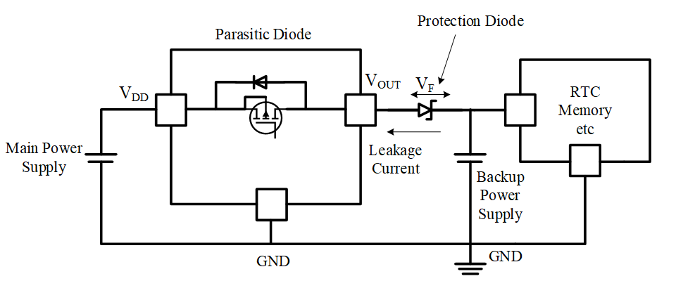
Figure 1: Leakage current flow in circuit
When there is an accidental (unwanted, parasitic) electrical connection between the floor and the conductor, the leakage flows. Whether the earth may be the zero-tension reference point or the earth. The real power unit leak should preferably reach the earth and ground.
Signal cables linked to other grounded or underground equipment, such as printers, are the most frequent source of current leaking in laptops or two-pin connections. When the other equipment is ground correctly, a channel is delivered to the earth; however, when it is not grounded correctly, anybody in contact with the metal exposed portions is shocked electronically.
Device leakages are generally caused by insulator failures or materials used to manufacture components such as semiconductors and condensers. In the case of a condenser, this results in a small amount of leakage or dielectric flow.
Reasons of Leakage Current
The isolation has both electrical strength and capacity, which allows the flow of current in both directions. Only a tiny amount of electricity should leak due to the high isolation resistance. However, the resistance decreases if the insulation is old and broken to allow much power to pass. A longer conductor also has a higher capacity, leading to increased leakage. Meanwhile, electronic equipment filters protect against power spikes and other disruptions. The presence of condensers on the input of the filter helps to the total capacity of the cable systems and the overall leakage current level.
Factors to Measure in Leakage Current
Leakage current can be measured in many ways, i.e., via parasitic pathways to the ground, leakage current through the ground conductor, and leakage current from the earth.
- Leakage Current via Ground Conductor: When the load is attached (on) it contains leakage current measured by leakage in loading equipment. The leak from the corded circuit is significantly smaller if the leakage is tolerable with the load attached. When cable leakage of the circuit is necessary, disconnect (disconnect) the load. Place the clamp around the ground wire to measure the total leakage of the proposed ground connection.
- Current Leakage to the Ground through Unintentional (Parasitic) Pathways to the Ground: The clamping phase identifies unbalanced current created by accidental ground paths on the outlet or electrical panel (such as the panel sitting on a concrete base). A similar imbalance may occur if there are other electrical connections (such as a connection to a water pipe). Figure 2 shows the schematic depiction of leakage current through unintentional paths to ground.
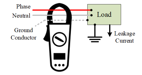
Figure 2: Leakage current via unintentional paths to ground
Leakage Current Estimation and Reduction Techniques
- The current source is identified as one approach to minimize the leakage current impacts.
- The use of an outlet current clamping meter is another approach. A clamp meter can detect and measure a large number of alternating and changing streams that run through a test leader. The number of leaks reported by a clamping meter can be significantly larger if telecommunication equipment is present than the level generated by insulating impedance.
- Power gating is used in an electric circuit to reduce leakage current.
- The scaling of supply voltage is used to decrease the circuit voltage. Scale the threshold voltage only with supply voltage and reduce circuit loss.
- Usually, the transient stacking effect reduces existing transistor leakage.
Leakage Current in ICs and Semiconductors
Sub-threshold currents and reverse diodes in a CMOS transistor in an ASIC, as well as semiconductor leakage power, waste a significant amount of energy. The leakage power of a CMOS logic gate is independent of the load capacitance transition; therefore, it remains constant for a logic cell. Although the voltage door is smaller than the voltage limit, the sub-threshold current passes via semiconductor devices from the source to the drain. This happens with a mild inversion because of the diffusion of the carrier between the CMOS transistor sources and drainage areas.
Leakage current is a significant conduction constraint of PN junction diodes. The width of the depletion region widens when a diode is reverse biased. Figure 3 shows the leakage current in case of transistor cross section. In general, this requirement is essential to limit the concentration of current carriers near the junction. Because the majority of current carriers are negated in the depletion region, the region behaves as an insulator. Current carriers do not normally travel through an insulator.
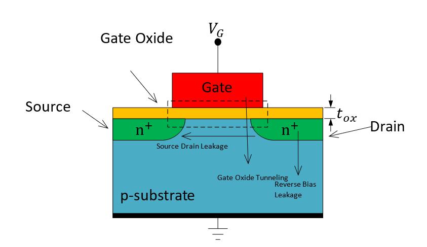
Figure 3: Components of leakage current in case of transistors


