Understanding LVDS (Low Voltage Differential Signaling)
03/10/2021, hardwarebee
Find electronic design, board design and module design companies:
Find FPGA design companies:
Find embedded software companies:
The most fundamental part of a communication system is the propagation media. It is where the signal is more prone to interference, distortion and attenuation. The propagation media can become significantly bulky and expensive in critical applications, that require high quality shielding and proper connectors. In this scenario, electromagnetic interference (EMI) is the main villain, being able to degrade the signal to the point of malfunctioning. Also, to obtain market approval from regulatory agencies, the electromagnetic compatibility (EMC) of your device must meet the required standards. To help solving this issue, the low-voltage differential signaling (LVDS) standard was developed, which can provide the EMI immunity with differential lines and is compatible with low voltage technologies. In this article, we will discuss the main concepts of LVDS, how it works, the applications and the advantages/disadvantages of using this technology.
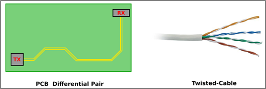
Figure 1: The main transmission media of LVDS: PCB differential and Twisted Wire
LVDS Basic Concepts
The working principle of the LVDS is simple: EMI is propagated in the air, so the amplitude of the signal is location dependent. This means that the closer two wires are from each other, the more similar is the interference experienced by both. Therefore, in a twisted pair configuration (showed in the figure below), the EMI coupled in each wire is basically the same, so the voltage difference between the wires is almost zero. This makes the differential voltage of the twisted pair much more immune to EMI than the single-ended counterpart. In LVDS, differential signals are used to transmit information, whereas the EMI is rejected as common-mode noise.
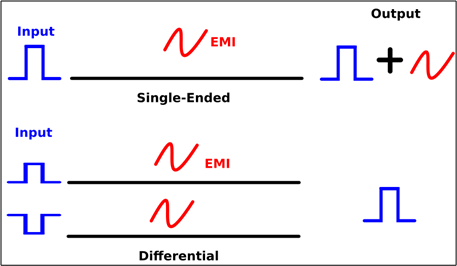
Figure 2: Difference single-ended signaling and differential signaling
To avoid confusion, LVDS is not a communication protocol. It is a technical standard that specifies how the signal should be transmitted, and any protocol can use this standard as a baseline technology. The LVDS standard states that the signal should be transmitted through a differential pair, and each line of the pair should have an identical voltage with opposing sign. There is, if 1 V differential signal is being transmitted, one line will have +0.5 V and the other line will have -0.5 V (for a common-mode voltage equals to zero). Therefore, the transmitter must have two identical injection outputs, and the receiver should perform a subtraction operation in the first stage.
In typical high-speed applications, a differential current is used instead of a voltage: each pair will carry an identical current (typically the same current flowing from and back to the transmitter), and this current generates a differential voltage at the receiver point (Figure 3). This approach not only improve performance, as current signals are less prone to losses and interference, but also reduces the emitted electromagnetic field, because the field generated from the forward current is being canceled by the backwards current.

Figure 3: LVDS basic implementation
LVDS Components
As in any communication system, the basic components of the LVDS are the transmitter, the receiver and the transmission line. The transmitter is responsible for injecting a current to the differential pair. This current leaves the transmitter from one line and enter the transmitter from the other line, with the polarity of the current defining the logic level. The transmitter consists of a constant current source, with typical value of 3.5 mA, and four MOSFET switches forming an H-bridge, as shown in the figure below.
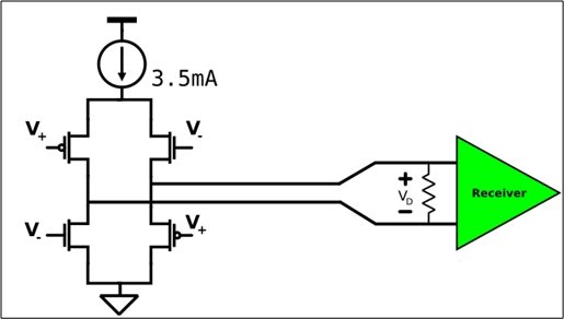
Figure 4: LVDS physical operation
The top switch of one line shares the control with the bottom switch of the other line, so they open and close together. Switches in the same line have complementary controls, so the polarity of the current passing through the differential pair can be controlled. The current then flows through a differential line, which can be implemented with twisted copper wires or differential paths in PCB.
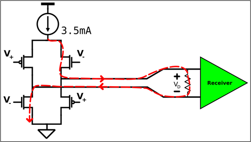
Figure 5: Current flow during one operation mode
At the receiver site, voltage passes through a termination resistor. The value of the resistor, which is typically in the order of 100Ω, should match the line impedance, to avoid reflections at high frequencies. When passing through the resistor, a voltage drop is generated at both receiver inputs. The receiver then subtracts the voltages to obtain the differential value. If 3.5mA and 100Ω are used, the voltage difference will be of only 350 mV, which allows very low-voltage applications. The common mode voltage of LVDS lines are typically in the range of 1.2V, but lower voltage applications may implement common-mode voltages as low as 400mV. Also, the LVDS standard tolerates ground shifts of ±1V between the transmitter ground and receiver ground. This shift, added to the common-mode transmitter voltage and the common-mode noise of the line, will result in the required common mode-range in the receiver.
Besides the basic topology explained above, LVDS can be implemented in different ways. For instance, the termination resistor can be divided in two, and added to a common mode RC circuit, to create an extra common-mode termination. Bi-directional operation is also possible, using two termination resistors (one for each receiver). Of course, only one transmission direction can be used each time, so when one device is talking the other should remain silent. The main disadvantage of this approach is that the resistors are seen in parallel from the transmitter output, which reduces the drop voltage and, hence, the noise margin. Multi-drop LVDS, also called LVDS bus, can also be implemented, where several different receivers can read from the same bus. Care should be taken when designing these circuits, as the transmitter should be able to drive several termination resistors.

Figure 6: LVDS with common-mode termination
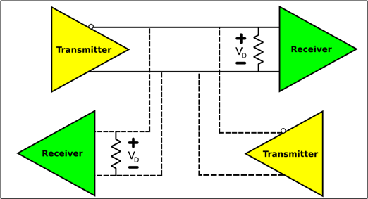
Figure 7: Bi-directional LVDS
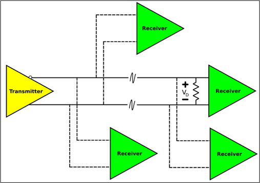
Figure 8: Multi-Drop LVDS
LVDS Standards
The most popular standard behind LVDS is the ANSI/TIA/EIA-644-A, which is defined by the American National Standards Institute, the Telecommunications Industry Association and the Electronic Industries Alliance. This standard defines output and input characteristics of transmitter/receiver, and recommends a maximum transmission rate of 655 Mbit/s, using twisted-pair wires. However this is outdated and several LVDS applications go to the Gbits/s range. Another popular LVDS standard is the IEEE 1596.3 SCI- LVDS, which is an technology standard for LVDS applied in Scalable Coherent Interface (SCI). This standard provides specifications for the signal levels concerning high-speed and low-voltage SCI, as well as data encoding.
LVDS Applications
LVDS is usually applied in high frequency data transmission systems. Computer buses, automotive electronics, video data transfer and LCD displays are the most prominent ones. However, LVDS can be applied in any transmission system that requires high-speed and cheap/reliable implementation. One of the first applications, and still one of the most popular ones, was the Flat Panel Display Link (FPD-Link). This technology is still an unofficial synonym of LVDS, and it is used to transfer video data from the graphics processor to notebook displays. This was a critical step towards computer miniaturization, as FPD-Link is able to reduce considerable the number of wires required for video interfacing. This approach was so successful, that LCD TVs begin to apply the technology into their screens. Other standards, such as the OpenLDI, are popular LVDS based methods for video signaling. LVDS is also used in vehicles for internal data transmission, being part of the navigation system, night vision and obstacle detection. This is because automotive applications have to work in an environment filled with EMI, so electromagnetic compatibility is a must. However, in this case, the twisted pair should be very well coupled, and a ground shielding should be used to reduce EMI even further.
Besides video signal transfer, LVDS can be applied in a range of high- speed communication buses. In fact, the IEEE provides a standard for LVDS applied to Scalable Coherent Interface (SCI). SCI is a standard for high-speed, point-to-point, and scalable shared memory microprocessing. LVDS is also being more and more applied in embedded applications that require critical EMC, such as biomedical devices and military technology, due to its robustness, reliability and cheap implementation.
Pros and Cons
The main advantage of using LVDS is the improvement of electromagnetic compatibility combined with low-voltage operation, which was well discussed in the previous sections. However, LVDS provides additional desirable features for high-speed transmission. First, the voltage compliance is doubled, because the signal is no longer limited to the single-ended output: for instance, if the maximum amplitude of each line is 1.65 V, then the differential amplitude is 3.3V (1.65V – (-1.65V)). This reduces the required supply voltage, which is desirable for low-voltage devices, and increases the SNR of the signal.
Another advantage of LVDS is the reduction of power supply noise: single- ended applications typically switch the output current polarity at high-speeds, which generates high frequency noise at the supply node. On the other hand, the output current of LVDS systems remains constant, with information being transmitted by the direction of the current. This reduces significantly the need for power-supply decouplers, which simplifies design and reduces the overall cost.
Compared to other differential signaling standards, such as positive-referenced emitter-coupled logic (PECL), LVDS provides a more scalable approach in terms of voltage. That is, LVDS can be easily adapted to small supply voltages while keeping the communication integrity and technological characteristics. However, it provides limited jitter performance when compared to other standards, such as PECL, and is also more costly. Moreover, it is more limited in terms of maximum supported data rate than other available techniques.
Conclusion
- LVDS is a differential signaling technology standard that can be used by different communication protocols;
- Differential signaling provides better electromagnetic compatibility, in- creases voltage compliance and SNR and decreases the minimum required supply voltage;
- LVDS also reduces the amount of supply noise currents;
- Compared to other differential signaling standards, it provides a reliable and cost-effective solution for high-speed data transferring, specially for video interfacing and automotive applications;
- LVDS can also be applied in low-voltage and compact embedded systems that require high EMC


